Part Number: TPS2663
Dear TI Support Team, I have a question about the PGTH function of the TPS26631.
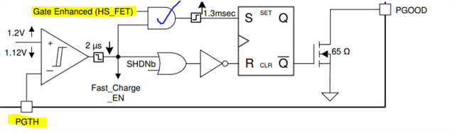
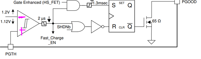
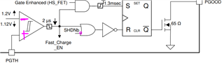
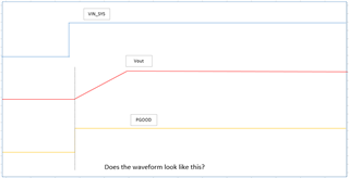
Are there any conditions for when PGOOD goes high at VPGTHR?
When PGOOD is low, does PGOOD go high when VIN = Vout instead of the set voltage by PGTH?
Thanks
Best regards,
Watanabe