Hello TI team!
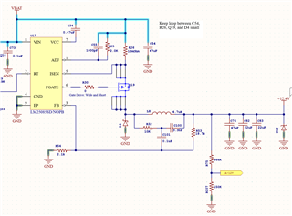
Here are the application details:
- Vin= 12.0 - 14.4V
- Vout= 12.4V
- Load= 5A
- Fsw= 300kHz
- 4 layer PCB (Signal 1, GND, PWR, Signal 2)
We have noticed that when our LM25085 regulator is switching, the digital circuits on our PCB start malfunctioning (LCD freezes, I2C communications get stuck, MCU internal ADCs give skewed conversions). The regulator itself functions exactly as expected and waveforms look normal.
The issues are very clearly only during switching. If Vin is less than 12.4 and the IC is operating with 100% duty cycle, the errors do not occur regardless of load current.
When it is switching, the errors don't seem to get any more/less severe depending on the load. The board is just as likely to fail at 100mA load as it is with 5A load. As long as it is switching...
As an experiment I replaced the 0-ohm gate resistor with 10-ohm and the malfunctions went away.
To me this suggests radiated noise from the switcher are disrupting the nearby digital blocks. Which is quite strange because oscilloscope captures of things like VDD and I2C SDA/SCL are quite clean.
I would like to ask the following questions:
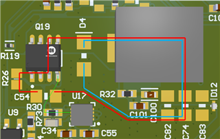
- Do you have any suggestions for improving layout? We tried to keep the loops small. Maybe it's not perfect but I wouldn't expect it to be so bad it breaks the system...
- What method is better for preventing high frequency emissions: gate resistor, switch node snubber, or other? I'm not sure which is best for this specific issue.
- Could the cause actually be something else? I'm worried the gate resistor was just a lucky cover up of a different issue... (It does seem the switch node under/overshoot improves with gate resistance).
Thanks in advance for your help :)
Schematic:
Layout:
(please excuse the missing models - they are not DNP, just no 3D models imported)
(red: ON loop; blue: OFF loop; green: gate drive)
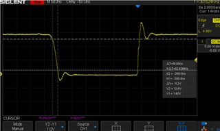
Switch node (0-ohm Rgate):
(19ns fall time; 6ns rise time)
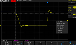
Switch node (10-ohm Rgate):
(45ns fall time; 11ns rise time)

