This thread has been locked.

If you have a related question, please click the "Ask a related question" button in the top right corner. The newly created question will be automatically linked to this question.

TPS23754: Primary FET damaged using Flyback topology.

Part Number: TPS23754

Hi sir,

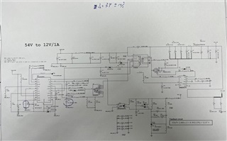
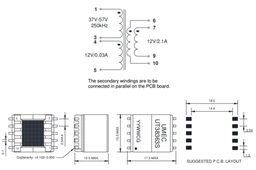
 We got the RMA issue from customer that we use TPS23754 PWM controller only with Flyback topology.

When customer use for a long period, sometimes we will get RMA back that primary FET, TPS23754 and current sense resistor damaged and can't turn on again.

After switching the damaged part and the unit can turn on again.

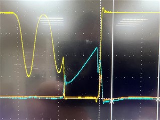
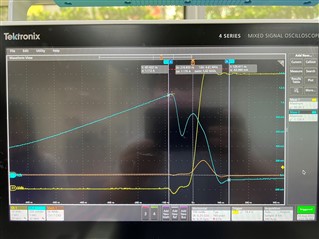
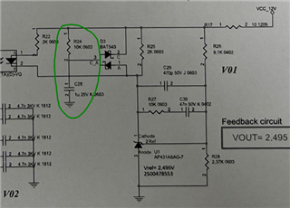
 Would you help to check the schematic and primary FET VDS, current waveform to see any clue for this issue? 

  • Hi Shihchin,

    Thanks for your question. Our team will try to figure it out. I have some questions for you:

    1.What does "RMA" stand for?

    2.Is the 3rd picture the zoomed-in picture of the 2nd one?

    3.Do you have the datasheet of the flyback transformer in the schematic (UT38363s)?

    4.Have you measured the temperature on the new primary FET?

    Best regards,

    Diang

  • 1. It means customer returned issue. This unit shipping to customer and using for a while, it back to our factory because of  the unit damaged.

    2. Yes. It's the zoomed-in waveform.

    3. Please see the below pictures.

    4. No we didn't measure it. I will ask our factory to check the temperature.

  • Hi Shihchin,

    Thanks for your update. Please let me know the temperature measurement results of that MOSFET.

    Since the damage happened at the MOFET and the current sensor resistor. I would first think about the rms current and device overheat issue. While, based on the waveform, the rms current seems less than 1A. Considering the 0.063 Ohm on-resistance, the conduction loss is less than 0.07 W. The switching off loss based on the zoom-in picture is about 2.7 mJ (54V * 1A * 0.5 * 100ns, a rough estimation). Assuming a same switching on loss, at 250 kHz, the switching losses is about 1.35 W.  So the total power losses could be ~1.42 W. With a 50 °C/W junction-PCB thermal resistance and a potential PCB-ambient resistance (depends on the pad size, seems this package does not have a thermal back pad). The temperature rise on that MOSFET could be more than 100 °C if the PCB-ambient thermal resistance is high. 

    By the way, since you are not suing GAT2, you could short DT to VB to disable the GAT2.

    Best regards,

    Diang

  • Hi Diang,

     Thanks.

    1. We will check the temperature of the MOSFET and XFMR. Once have the data will share with you.

    2. Actually we already short DT to VB, you can see the schematic DT pin with the VB wording on it.

    3. Do you have the suggested XFMR data or spec. for us to see how to improve this issue?

  • Hi Shihchin,

    Thanks for your response. Sorry that I missed the VB label in your schematic. 

    The flyback transformer you used has 37 uH mutual inductance, which shows a peak-peak current close to100% of the dc current as shown in your waveform. I think using a flyback transformer with larger mutual inductance (50 - 100 uH probably) could reduce the rms current and switching-off current to potentially lower down the MOSFET power losses. 

    I would suggest running the temperature measurement first. If the overheat really exists, we can locate it and will try to solve it.

    Best regards,

    Diang

  • Hi Diang,

     We measured the FET temp. in room temper and the temp. is about 66 degree C. So the temp. of FET is not really higher.

    Do you have other idea for this issue?

  • Hi Shihchin,

    Thanks for the test results. Seems at normal operation, thermal is not the major issue to cause the MOSFET fail. But your case is not an instant failure, it still possible at some working conditions, thermal could kill the MOSFET.

    Another reason could be the critical electrical field. May I know the failure mode of the primary MOSFET? Is the gate to source oxide failure, drain to source breakdown, or others?

    1. Gate to source oxide failure: for some reason, if R20 and R21 fail first, then the turn-on source voltage is close to the drain voltage, while the gate voltage is refer the RTN rather than source. So the Vgs voltage could exceed the limitation and breakdown the gate to source oxide.

    2. Drain to source breakdown: for some reason, if the voltage overshoot is higher than the 150-V rated voltage at some operation conditions, the MOSFET may have insulation failure or degradation.

    You can use a curve tracer to do a static measurements (1st quadrant I-V, 3rd quadrant I-V, Idss, Igss, Vth) on the failed device to know its failure mode. 

    Best regards,

    Diang

  • Hi Diang,

    One question about the CS pin when soft start period. When soft start period, if CS pin trigger the Vcsmax. Will it start to trigger the current limit? or CS pin will skip it until softstart completed?

  • Hi Shihchin,

    PRI side has ~4 ms soft start time and the SEC side also has the soft start circuit shown below. Normally during the soft start, the duty cycle is limited.

    The CS pin trip level ramps from 0V at the beginning of soft start to 0.55V typically after 3.9 ms. The pulse can also be terminated during soft start when the CS voltage reaches the trip level between 0V and 0.55V. With the 0.75V offset, the PWM comparator input ramps from 0.75V to 1.3V.

    Best regards,

    Diang

  • Hi Shihchin,

    Since your question has been answered, I will close this question for now. If you have any further questions, please open a new thread and we will be glad help you!

    Best regards,

    Diang