Hi team
There is a good new that we DIN LMR36503MSC5RPERQ1!
Please help confirm the SCH and Layout is ok?
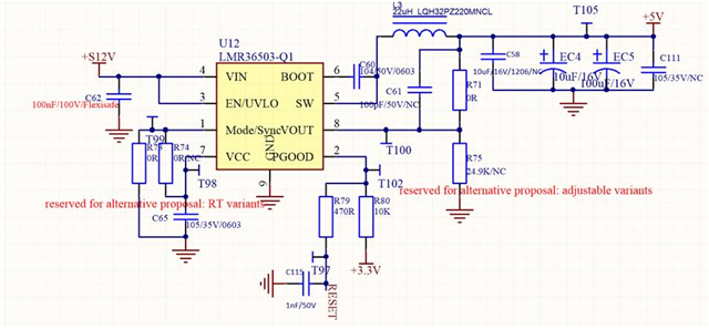
1.SCH
2.Layout , U12 on top layer is DCDC IC
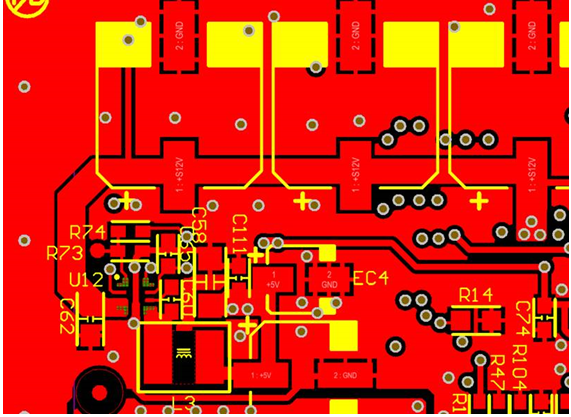
2 layers are ground

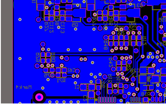
3 layers

4 layers of wiring
This thread has been locked.
If you have a related question, please click the "Ask a related question" button in the top right corner. The newly created question will be automatically linked to this question.
Hi team
There is a good new that we DIN LMR36503MSC5RPERQ1!
Please help confirm the SCH and Layout is ok?
1.SCH

2.Layout , U12 on top layer is DCDC IC

2 layers are ground

3 layers

4 layers of wiring

Hi Kygo
The schematic is ok, except that a 10uF ceramic capacitor between Vin and GND of U12 should be added, and should also be placed near the Vin & GND pin.
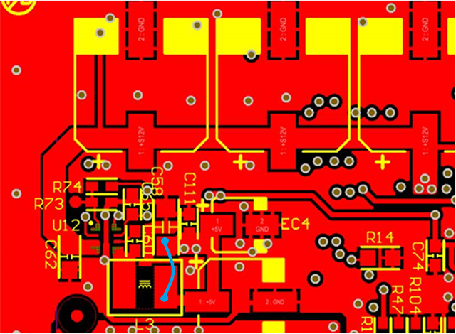
For the layout, I think the connect trace between L3 and C58 can be shorter.
Best regards.