This thread has been locked.

If you have a related question, please click the "Ask a related question" button in the top right corner. The newly created question will be automatically linked to this question.

TPS7A8300: Temperature stability and solder profile in RGW (5mm x 5mm) package

Part Number: TPS7A8300
Other Parts Discussed in Thread: ADS54J66

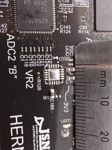
We have been searching and waiting for available components to complete our project and found demonstration boards with the desired TPS7A8300RGW package.     We noticed that once installed on our boards, these regulators no longer provided stable output and are highly sensitive to temperature.   We never experienced this issue while using the 3.5mm package TPS7A8300RGR.    Those smaller chips were routinely removed, swapped and returned to function during our development phase.    Only when we switched to the larger *RGW package have we experienced any issues with performance.    The demonstration boards function extremely well and exhibit no temperature sensitive behavior.   Once the chips are removed, they suffer in performance.

We did a series of experiements, including thermocouple measurements during removal and installation, removal and immediate re-installation on the same demo board and even wiring and testing VIN, ENABLE, and VOUT (with decoupling capacitors) while the chip was unmounted and loose.

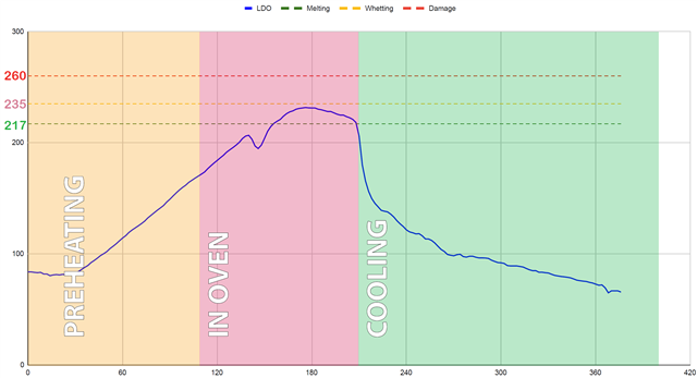
During all our Pb-Free soldering processes, the temperature never exceeded 260'C.   This complies with warnings and optimal profile found in the QFN attachment application note SLUA271B  Our installation profile looked like this

In all cases, the LDO mounted to the demonstration boards worked well while any other mounting was sensitive to temperature increase.   Specifically, blowing on the chip causes VOUT to rise, settling back to the specified VOUT voltage (1.15 in our case).

We're stuck trying to understand what could be harming these devices, and why they function well on the demo boards but fail as soon as the solder reflow occurs.

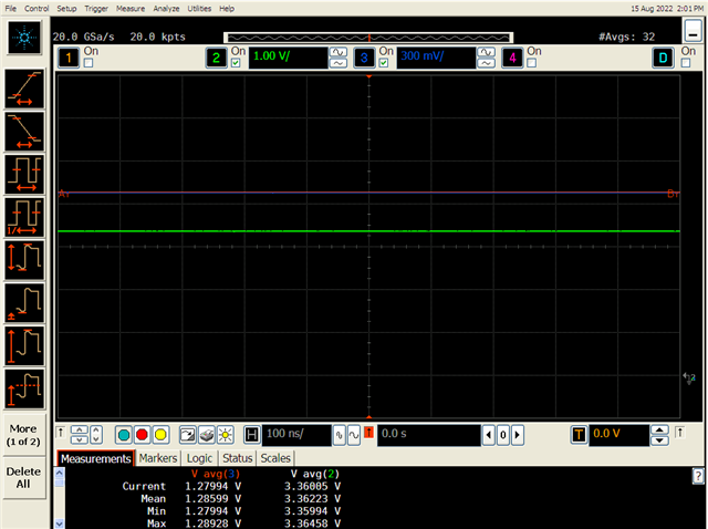
Demo board before reflow:  (Blue : 3v3 VIN, Green : 1v15 VOUT)

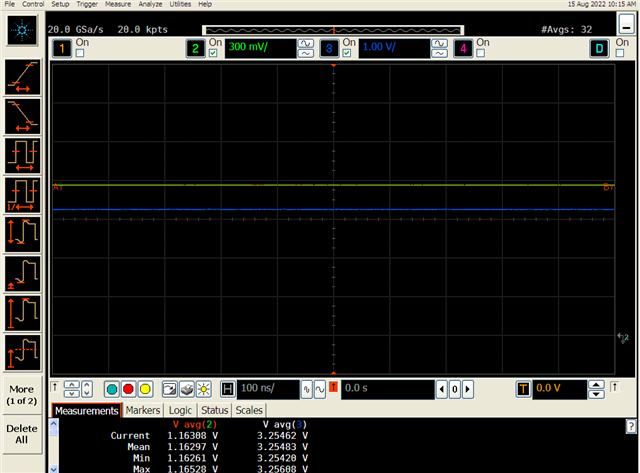
Demo board after reflow: (  Blue : 1v15 VOUT, Green : 3v3 VIN...swapped leads )

  • Hey Jon, 

    please give me 1-2 business days to look into this thread. 

    Best,

    Juliette

  • Hey Jon, 

    I have some questions before I can move forward:

    - What is your load current? Is this load being applied to the demo board as well?

    - Do you have similar connections seen on the demo boards  on your application boards?

    - When you reinstall, is the issue seen on both the demo board and your application boards?

    - Is the thermocouple testing ambient or is it attached to the part?

    Best,

    Juliette

  • Thank you for looking into this.   I have some information that might help.   We are providing the core voltage for a pair of ADS54J66 chips and this worked nicely on prototypes and our first three revisions of production boards.    We made a handful of spare boards and changed from the 3.5mm package to the 5.0mm package hoping for better thermal behavior.

    Load Currents:

    The load current for the chip on a fully populated application board is around 1 amp.  1.066 A by rough estimate.   I applied a load current of 14mA to the demo board and it worked very nicely.

    Connections:

    The connections on the demo board and our application board are very similar.  Both circuits have robust thermal pads below the device, with via-in-pad contacts to a ground plane.  Both circuits are using the AnyOut pins to set an output voltage of 1.15V in both circuits.   This is achieved by grounding pins 5, 6, and 7 (50, 100 and 200mv input)   Both boards tie pin 14 (ENABLE) to VIN for always on function.    Both boards tie pin 2 (SNS) to VOUT to read the output directly.   Both boards use a feedforward capacitor from VOUT to stabilise pin 3 (FB).    Both boards use a capacitor to fix the slow start feature on pin 13 (NR/SS).

    Our application board includes 3.0v on pin 12 (BIAS) and the demo board does not.

    Reinstallation:

    I tried removing and installing the chip on an application board.    I also tried removing and immediately re-installing the chip on the same demo board it came from.   

    Thermocouple:

    In the solder profile images above, the thermocouple was directly touching the top surface of the LDO chip during the hot-air removal process.   The same thermocouple was as close as possible to the chip during re-installation.   I didn't want to disturb the solderpaste with contact.   The included picture shows the thermocouple placement during the 'immediate' re-installation on the same demo board mentioned above.

  • Hey Jon, 

    Just in case - is the RGW being populated on the RGR footprint?

    Potential Issues:

    - Leakage on ANY-OUT Pins

    A method of troubleshooting this is  by cleaning off the board after the solder process to remove any flux. There may be leakage current on the ANY-OUT pins.

    - Poor connection on power pad:

    Measure the THETA-JA on a new EVM afterwards check the THETA-JA on a reflowed board to see if maybe there has been an issue connecting the Power pad. 

    Best,

    Juliette

  • Leakage and cleanliness:

    We use lead free solder paste in a water-based flux routinely.    For this set of tests, our boards were cleaned using DI water, then dried over hours.   Once clean and dry, the board was heated using either a hot air rework nozzle (temp chart above) or in the case of evaluation boards, heated from below with a hot pad.

    The resulting chips and boards were cleaned again, then paste applied and re-flowed in our IR convection oven (temp chart above).    Water based flux is used to remove any solder bridges and the installed chips are again cleaned with DI water and dried over hours.     It may be possible that there is leakage current on the AnyOut pins, but I am confident it isn't due to a lack of cleanliness.

    Poor Connection to Power Pad:

    The poor connection to the power pad is a possiblity.   It is, of course impossible to inspect or measure the thermal pad after the chip is installed.   I am eager to measure the θJA and compare a new EVM to our boards and to a 'remove-and-reinstall'd EVM but not sure how to go about this.   From what I have read, θJA is determined by θJA = (TempDieJunction - TempAmbient) / PowerDissipated.    I can easily measure the ambient temperature and calculate the power draw demanded of the LDO chip.   How do I best measure the die junction temperature on the EVM?   Is there an integrated thermal diode in the TPS7A8300RGW?    How would I access it?

  • The chip is indeed targeted for a QFN65P500X500X100-21N decal which should match the RGW package of this chip.

  • Hey Jon, 

    We have this app note that helps walk you through measuring thermal performance. 

    Measuring the Thermal Performance of theTPS54620

    I will keep looking into potential issues if it is not a power pad connection issues. 

    Best,

    Juliette

  • Hey Jon, 

    I am going to mark this as closed. Please respond if you are still having issues. 

    Best,

    Juliette