Hi,
My customer has two questions of Layout. Could you please answer them?
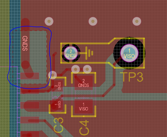
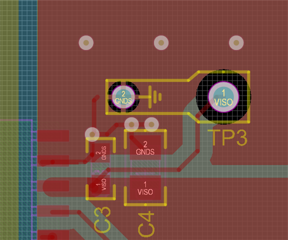
- According to 10.2 Layout example on the datasheet, TP1 for VINP is routed under C1 capacitor, and TP3 for VISO is routed under C4 capacitor. He seems not good pattern on these lines. Could you please let us know the reason why these are routed under capacitors? My understanding is priority of TP routing is lower than other lines. Is it correct? Please let us know.
- On this layout example, routing of #16 GNDS pin is longer than one of #15 GNDS pin. How long line is routed from #16 GNDS pin to GND plane? In other words, How far between #15 GND pin and C3 GND? Please advise us.
Thanks and best regards,
M.HATTORI.