Other Parts Discussed in Thread: TPS61022, TPS63802, TPS61023
Hello,
We are looking for a boost converter with following specifications:
Vin = 5.20V to 1.50V
Vout = 5V , 200 mA
The input voltage of the boost converter (Vin) is the 5V external power input of a video processing module.
The output of the boost converter is used to supply power to electronics that must work properly during the ramp down of the input voltage (non-planned power input loss)
Our target is to still have 5V (with 200 mA source capability) until Vin reach 1.5 Volt.
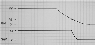
In regular operating condition (outside power down phase), the input and output voltage will be approximately the same.
But, due to the tolerance on the Vin voltage and accuracy of the boost converter output, we could be in different situations:
Vin > Vout (for example Vin = 5.2V and Vout = 4.9V )
Vin < Vout (for example Vin = 4.8V and Vout = 5.1V )
We could be satisfied with a pass-through mode in case of Vin > Vout, but we need a clean output in all conditions without big ripple due to change of operating mode of the converter.
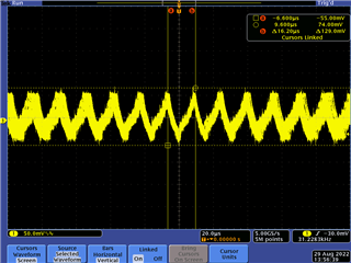
Test of TPS61202:
We have evaluated the TPS61202 component (Eval board).
With this component, as long as Vin is lower than 4.8V (for Vout = 5V), everything work perfectly and the output voltage ripple is quite good.
But, for Vin = 4.9V or 5V or 5.1V, we get very high ripple at the output ( -> more than 120 mVpp at quite low frequency 60 KHz)
TPS61202_VIN-5V_VOUT-5V_200mALoad_MultiTrace (cursors: delta T = 16uS, delta V = 120 mVpp)
TPS61202_VIN-5V_VOUT-5V_200mALoad_SingleTrace (cursors: delta T = 16uS, delta V = 120 mVpp)
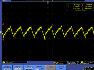
The state of the mode pin does not change anything, the component seems to work in a kind of PFM mode with high amplitude low frequency ripple.
Do you believe that the behavior observed were normal for this component or is it a defective EVAL board?
With this component, do you believe that it will be possible to get a low ripple at the output when Vin is close to Vout?
We have tried to put a bigger capacitor at the output (680uF OSCON) to reduce the ripple, but by doing that we have finally destroyed the component (after failure: almost short circuit at the Vin pin of the TPS61202)!
During the last test made (before failure), I have (most probably) connected during operation, a discharged capacitor (680uF 22mR) to the output of the converter!
But, I am surprised it will be sufficient to destroy the component, the component does not seems very robust to this kind of stress.
Any comment about that ?
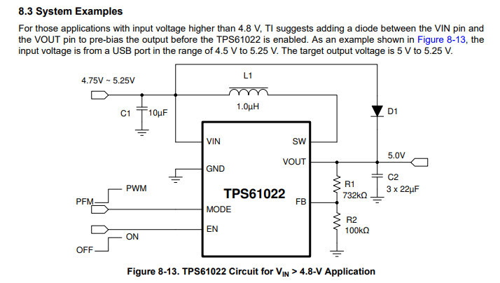
TPS610022:
We have also identified the TPS61022 as a possible candidates for this converter.
We have not yet evaluated this component.
But, for this component we can read this remark: Vin = 0.5 to 5.5V -> Output voltage pre biased > 0.7V before start-up
On the TPS61022EVM schematics we can read Vin = 0.5 to 5.5V but, no diode present for output pre-bias, what is the consequences to not have a pre-bias (no start up, stress in IC...)?
TPS63802:
We have also identified the TPS63802 as a possible candidates for this converter.
We have not yet evaluated this component.
For this component, what about the risk to have ripple due to change of operating mode boot/buck-boost/buck (even if we can read in datasheet: The device provides a seamless transition between all modes).
What are the Vin transition values between the 3 modes for a 5V output?
What is the best candidate for our use case?
Any comments and suggestions will be welcome
Thank you for your support