This thread has been locked.

If you have a related question, please click the "Ask a related question" button in the top right corner. The newly created question will be automatically linked to this question.

LM5060: Design review

Part Number: LM5060

Hi Team,

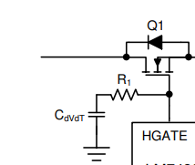
A customer is using this device as a highside NMOS switch.

However, the high side output does not turn on the NMOS. The voltage on OVP, UVLO, EN and are all ok but the nPGND and Timer is around 5.5V.
They tried to increase TIMER caps to 1uF but it does not help. When the TIMER pin is connected to GND the NMOS turns on when no load but when connecting high capacitive load output had not rise above 3.5V.

I hope you can check. Thank you for the help.

Regards,

Marvin

  • Hi Marvin,

    Please remove R1 and check once. It might be loading the GATE.

    Best regards,

    Rakesh

  • Hi Rakesh,

    The customer removed the R1 and it worked. However, the MOSFET is damaged and resulted in shorted constant load ON.

    The customer is building a protection switch between 55V battery and motor ESC (electronic speed control) circuit. The battery had about 49V while testing. ESC has high input capacitance with 6x470uF capacitors, due to which high inrush current is present at startup.

    They have tried switching the switch without the load and this functions great with 2.5ms rise time. To check if inrush is the problem they also added 48 ohm series resistance to the ESC and measured 4ms rise time and the switch was functioning normally.

    Should a limit in inrush with changing gate resistance and capacitance to increase mosfet rise time?

    Regards,

    Marvin

  • HI Marvin,

    While starting up with load into huge capacitance, the total current flowing through FET will be = Inrush current to Charge the output Capacitance + the load current. This current multiplied by the different of Input and output voltages will create a power loss in the FET (= (Icap + Iload) x (Vin-Vout)). If the power dissipation is greater than what the FET can handle (Safe Operating Area), the FET can be damaged.

    Here we would recommend to consider the following,

    1. Add a R and C in series from FET GATE to GND. These components will form the dvdt circuit and limit the inrush current during startup. You can start with values of R1 = 10 ohms and Cdvdt = 47nF
    2. Enable the load only after the Vout ramps up to Vin. This will remove the Iload component from FET power loss during startup. 
      1. After successful startup, the Vout will be = Vin, which means the Voltage across the FET is approx. 0V and hence the power dissipation in the FET will be very low ( = Iload2Rds(on)).

    It is very critical to ensure that the FET power loss is within the FET SOA to ensure the FET does not gets damaged. 

  • Hi Praveen,

    Thank you for the recomendation.

    I have addtional question about OUT resistor - R9 in the schematic. Is this needed or can be removed? I see it could be important is when battery gets disconected and there is sufficiant voltage present on ESC due to high input capacitance. These cases occure when battery can be manualy disconnected or if overcurrent is triggered and BMS switches off the battery.

    Regards,

    Marvin

  • HI Marvin,

    The value of R9 needs to be calculated based on the below equation.