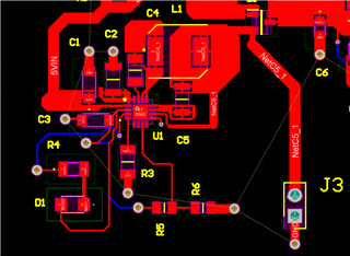
Hello,
Please review my pcb layout.
I have not made a ground polygon pour yet to connect all ground connections due to difficulty seeing traces and components after pour on the bottom layer.
Thank you,
Andres Perez
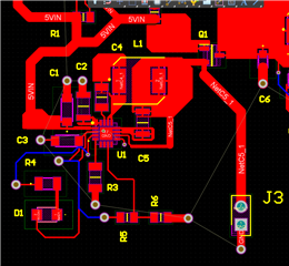
Hello,
Please review my pcb layout.
I have not made a ground polygon pour yet to connect all ground connections due to difficulty seeing traces and components after pour on the bottom layer.
Thank you,
Andres Perez