This thread has been locked.

If you have a related question, please click the "Ask a related question" button in the top right corner. The newly created question will be automatically linked to this question.

UCC27710: Power management forum

Part Number: UCC27710


hello.
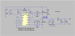
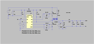
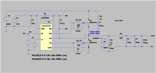
I am considering a chopper output circuit using UCC27710.
The switching element uses a bipolar transistor to reduce noise.
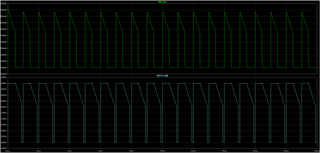
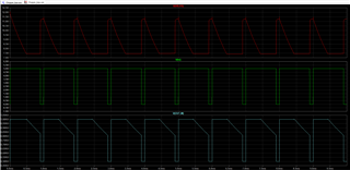
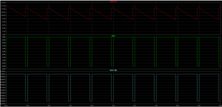
I'm using. When you operate it, the base current will drop from the middle,
The output voltage will drop.
Is there a current limiting circuit on the HO output of UCC27710? if there is
What is the upper limit current?
Thank you.

  • Hi, 

    Thank you for your question. Could you please specify in the schematic where the green signal and blue signal are being measured?

    Best regards,

    Leslie

  • Hi,
    Green is the current in resistor R7 connected to HO. The current becomes 0 in the middle.
    Blue is the OUT-M voltage of the output. The question is, is it due to the current limit on the HO terminal?
    If so, what is the current limit?
    Thank you.

  • Hi, 

    Thank you for the clarification. How long is the HI input pulse staying high? the reason I ask is because the HO output is biased by the external capacitor connected from HB to HS, and the capacitor relies on the switching of the low side transistor to recharge on each cycle. What could be happening is that the capacitor is discharging below HB-HS UVLO threshold and therefore HO is dropping to 0 before the cycle is complete. I recommend to measure the HB-HS voltage level with a differential probe to check if the voltage level is going below HB-HS UVLO threshold. 

    Regarding your questions about current limit, the driver is design to drive a capacitive load and therefore is able to deliver a peak current of 0.5-A source, 1.0-A sink. The abs max spec for DC current at the output is 150mA. However, the driver is not able to be 100% of the time on at HO since the capacitor biasing the high side driver will discharge and eventually reach UVLO. 

    The output current is limited by the output stage of the driver, FET internal resistance and any added gate resistors (more info here: https://e2e.ti.com/support/power-management-group/power-management/f/power-management-forum/1105985/faq-ucc27614-gate-driver-peak-current-considerations).

    Best regards,

    Leslie

  • hello.

    Thank you very much for your quick reply. The HI input pulse (green in the graph) is 900uS. Between HB and HS (red in the graph) was below the UVLO threshold at 500uS as indicated in the answer. I understand about the current limit. As an improvement plan, I changed the base resistance of the transistor from 2kΩ to 10kΩ because the output current is 1mA. The results are shown in the attached graph. The lower limit voltage between HB and HS is 9V or more, and the output voltage did not drop. If there is no problem, I will keep 0.47uF of C1 and adopt this circuit. If you have any comments, please let me know. thank you very much.