This thread has been locked.

If you have a related question, please click the "Ask a related question" button in the top right corner. The newly created question will be automatically linked to this question.

TPS54560B: TPS54560B

Part Number: TPS54560B
Other Parts Discussed in Thread: TPS54560,

https://drive.google.com/file/d/1Wl4QeXNmdnPTEHqAqKZgJTs-wI_8RmnF/view?usp=sharing

Too much heat is generating over the board and the IC Temperature goes beyond 94.2 Degrees with normal load and 105 degrees with 70% switching load 

Load Type : 72W LED


Result-1 :
Too much heat is generating over the board and the IC Temperature goes beyond 94.2 Degrees
Load Type : 72W LED Connected with MOSFET and 75% Dimming@ 14KHz PWM frequency


Result-2 :
1. Temperature further shoots up to 102.4 degrees
2. Humming sound is coming if we decrease MosFet Switching frequency below 12 KHz

Test Conditions:
1. IP67 based enclosure design , No Wind or Air Circulation for the IC cooling
2. Ambient Temperature of the LAB : 28 degrees
3. Readings are taken from Thermocouple ( Placed over the TPS54560 IC)
3. All reading are with Box Lid is closed
4. Used MosFET to drive the LED LOAD in Test condition-2 

Requesting E-2-E Community to please advise on this, how to further reduce the heat generation

  • TPS54560B Test Results are attached in the Link 

  • Hello,

    Can you provide the actual pdf of your test results as an attachment in this e2e post?

    Additionally please provide both schematic and PCB layout for further review. 

    Regards,

    Jimmy

  • TPS54560B Test Results.pdf

    Please find the attached file which contains all of the requested information including the PCB Layer files. 

    Please note that this is 4Layer PCB board with inner Cu thickness of 35Micron and outer thickness of 60 micron

  • Hi,

    Thank you for the attachment. I will need to spend some time to thoroughly go through this and review the file.

    I will provide updates with feedback once I get through the file.

    Regards,

    Jimmy

  • Hello,

    Given that this is only a 4 layer PCB, I think it would be good to have all 4 signal layers to have 2oz Cu which comes out to be roughly 2.8mil thickness. 

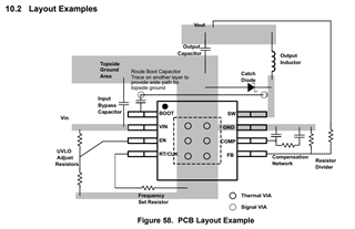
    For this high output power (72W) design, it would be important to have multiple GND thermal vias to help stitch the inner layers to the top and bottom layer for added thermal performance. Primarily the PowerPAD should be connected to the internal PCB ground planes using multiple vias directly under the IC, see example layout below:

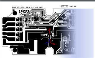
    Also how big the the total solution. It looks like having the "edge connector" on the left side of the board cuts the GND plane such that top layer heat is bottlenecked and can only flow through the red arrows which have minimal GND. Without the inductor on the left side blocking the path, heat flow would also move through blue arrow. 

    It may also come down to requiring a bigger board to lower the board resistance to help with thermals. Larger board area allows for heat to radiate further out of the IC package and cool the part.

    Regards,

    Jimmy