This thread has been locked.

If you have a related question, please click the "Ask a related question" button in the top right corner. The newly created question will be automatically linked to this question.

LM5118: Can LM5118 operate in only Buck topology and unpopulate the Boost low-side MOS?

Part Number: LM5118

Hi team,

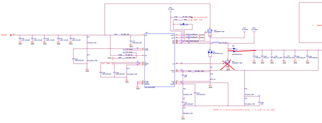
The customer used LM5118 as 12Vin-12Vout before, but now the input voltage changed to 24Vin, minimum 16V, and 12Vout, can any components be unpopulated and operate LM5118 as a pure Buck topology?

Thanks!

  • Hi Bryce,

    Thank you for using E2E forums, I think depending on the BOM some components might need to be changed depending on their rating values as the Vin maximum has doubled so i would guess the input capacitors and the MOSFETs as well, but again depends on the rating of the components. 

    Also, it goes without saying that in order to facilitate this change in the Vin some part of the design needs to be altered to facilitate the Vin range and this is explained in the datasheet and quickstart calculator here https://www.ti.com/product/LM5118#design-tools-simulation

    Hope this helps,

    BR,

    Haroon

  • Hi Haroon,

    Thanks for your feedback, what I mean is can I remove Boost low side MOS and short Boost rectifying diode to make it work in only Buck mode?

    Regards,

    Bryce

  • Hi Bryce,

    Thank you for your reply, as you can see here in this thread https://e2e.ti.com/support/power-management-group/power-management/f/power-management-forum/1099109/lm5118-using-lm5118-in-boost-only-topology it might not work as the usage of LM5118 in boost only did not work. I could try to recreate your suggested schematic but it might take some time.

    BR,

    Haroon

  • Hi Haroon,

    Thanks for your feedback.

    It's understandable for me that pure Boost may not work properly since the current sensing doesn't work well. But I am not sure if Buck can work since all sensing signals can be sensed into the control logic. So would you please try on EVM? I think the schematic doesn't need to be same, just remove the Boost low-side MOS is ok.

    Thank you very much.

    Regards,

    Bryce

  • Hi Bryce,

    Understood, please allow me some time to get back to you on this, I will recreate this in the lab and get back to you in a day or two.

    BR,

    Haroon

  • Hi Bryce,

    Thank you for your patience, regarding your query after trying out what you had asked the output would go up to the desired value and switching would start but as soon as the Vout hits the desired value the switching stoped and Vout dropped to zero and after a while the same thing would repeat. I guess in the startup it does not go to buck mode and hence the output drops.

    BR,

    Haroon

  • Hi Haroon,

    Really appreciate!

    I still have some questions need to check, why the switching stopped once Vout reached the target value? Does it trigger some protection or some other reasons? Do you have some scopes about the test waveforms like SS, Vout, COMP, iL, SW?

    Thanks!

    Regards,

    Bryce

  • Hi Bryce,

    Very sorry for the delayed response I was out from the office. The Vout never reaches the target value, the device just stops switching and then the Vout is disconnected from the input hence it drops to zero as well. I am not sure if that is due to some protection triggering would need to check further.

    I will do some more tests and send you the waveform.

    BR,

    Haroon

  • Hi Haroon,

    Thank you very much for your feedback, looking forward to your more waveforms.

    BRs,

    Bryce

  • Hi Bryce,

    So I re-did the test and first time the normal operation of the device in buck-boost mode 20V vin to 12V output.

    C1 is SW1 for the Q1, C3 is SW2 for Q2, C4 is Vin.

    After removing the Q2 to run the device in Buck only mode:

    C1 is SW1 for the Q1, C3 is SW2 for Q2, C4 is Vin and C2 input current

    Here the blue waveform is also the output voltage and as soon as the output hits the 12V it drops to 8 V same as the SW1 or C1 that also drops to 8V and both of them stop switching.

    Here are the SS and COMP pin waveforms as well, they have a lot of noise due to no proper points of measurement of the two pins.

    C1 is SW1 for the Q1, C3 is SW2 for Q2, C4 is Vin and C2 is COMP pin.

    C1 is SW1 for the Q1, C3 is SW2 for Q2, C4 is Vin and C2 is SS pin.

    Hope this is helpful.

    BR,

    Haroon

  • Hi Haroon,

    Thanks for detailed waveforms, the result is confirmed that LM5118 cannot be used as pure Buck topology. And from the waveforms, it can be seen that SS pin didn't restart, COMP is high clamped. It seems that some protection is triggered.

    Thank you very much for your help, really appreciate.Blush

    BRs,

    Bryce