This thread has been locked.

If you have a related question, please click the "Ask a related question" button in the top right corner. The newly created question will be automatically linked to this question.

TPS548D21: Circuit review for EMI/EMC

Part Number: TPS548D21

Dear TI Team,

We are using TPS548D21RVFT power regulator IC in our new project and it will be used to supply core voltage of main processor on the board(0.8V @ 40A). This is a mass production version of board and we are doing EMI/EMC compliance tests for this board. So by considering this, what and all improvements/ corrections we need to take care in the current design. Also request you to review the attached schematics and provide your feedback.

Best Regards,

Vyshnav Krishnan

TI_TPS548D21RVFT.pdf

  •  

    We are not EMI / EMC compliance experts, and EMI / EMC compliance depends heavily on factors outisde of the DC/DC switch mode power supply schematic, but we can provide some general guidance in design considerations to reduce conducted and radiated noise.

    1) I would recommend incrasing the VDD to GND filter capacitor from 0.1μF to 1.0μF or adding a 1.0μF capacitor from VDD to GND

    This is not an EMI/EMC compliance issue, but a device operation issue.

    2) I would recommend including an intermediate input capacitor value between 22μF and 10nF.  While the 10nF capacitor will generally help suppress the 50-200MHz switch node ringing frequencies generated by the resonance of the switching node, a 10μF or 4.7μF capacitor in parallel with the 22μF capacitors will help suppress lower frequency noise.

    3) Since the Ferrite Bead (L16) will prevent VCC_3V3 from sourcing dynamic current into 0V8_REG_IN during a load transient on the output, you might want to consider some additional input capacitance to support VIN during dynamic loading of VOUT.  This, of course, depends on the dynamics of the loading current, so if you have tested this design with L16, this may not be necessary.

    4) As with the input voltage, I would recommend some low value (0.01μF / 0.1μF / 1.0μF)  output capacitors to provide a low-impedance for high-frequency noise conducted through / around the inductor to the output.

    5) Once you have your board, I suggest following the attached procedure to optimize your snubber value:  https://e2e.ti.com/blogs_/b/powerhouse/posts/calculate-an-r-c-snubber-in-seven-steps 

    Snubber_Calculations.xlsx

    Most of your EMI / EMC improvements will be with layout design.  Here are some general recommendations:

    1) Minimize the size of the switching node.  It should be large enough to provide conduction from the SW pins to the inductor terminal, but no larger.  The corners should be rounded or chamfered at 45 degrees rather than 90 degrees.

    2) The spacing between the Switching Node and the Output Node should not be closer than the inductor pads to avoid increasing the parallel capacitance across the inductor and high-frequency conduction from Switching node to Output Voltage

    3) Input and Output Capacitors should have multiple vias to ground planes as close to capacitor terminals as design rules allow to minimize parasitic inductance.

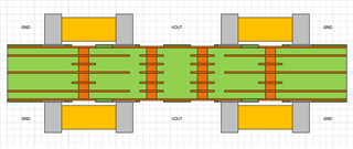
    4) Laying two capacitors end to end with VOUT between them and GND on opposite sides will provide a lower impedance ground path than laying them side by side.

    5) If capacitors can be placed on both sides of the PCB, mirroring this configuration on top and  bottom with multiple GND and VOUT vias will significantly reduce parasitic inductance and high-frequency output conducted noise.  This replicates a Feed-through capacitor in a PCB design.

  • Dear Peter,

    Thank you so much for detailed explanation and suggestions. We will take care the same in design.

    Thanks & Regards,

    Vyshnav Krishnan