This thread has been locked.

If you have a related question, please click the "Ask a related question" button in the top right corner. The newly created question will be automatically linked to this question.

Please help with this TPS5450 set up.

Other Parts Discussed in Thread: TPS5450

Question1:

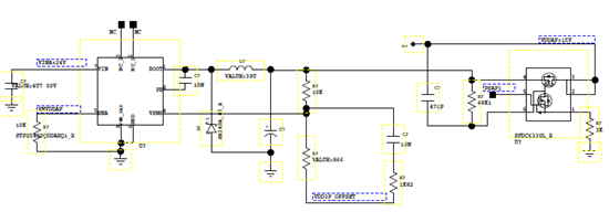
In my design, I plan to use DAC to adjust the output of TPS5450, do you think my RC compensation network should be connected with DAC output as in attachment image or RC network should be connected to GND?

Question2:

Since on the design, there are five of this TPS5450s working in parallel to power each its load, but I have used one DAC output to tune those five offset, I want to connect a buffer between the output of DAC and the low side of TPS5450 resistor divider.

 Please help me to see if my follow idea is correct:

DC Current for each TPS5450 resistor divider = 15V/10K+866 = 1.3mA

AC current for each TPS5450 resistor divider = 50V/10K+866 = 4uA

The total current for each TPS5450 resistor divider = 1.304mA

The total current for five TPS5450 resistor divider = 6.52mA

Based on those result, I need a buffer can sink at least 7mA.

Please correct me if I am wrong.

Thanks and Best Regards.

  • So sad, no answers....

  • David,

    There's been a formatting problem with this post.  The HTML formatting results in your post displaying just blank.  And we can't help you if we can only see a blank post.  I had a moderator correct the formatting so now it reads properly.

    In the future, please use the 'paste from word' icon in the header menu to enter/paste your questions.

    I would connect the RC to ground.  But this has not been tried/tested, so you can experiment with both configurations and see which works best.

    It's hard to read your schematic values (pdf would be easier), but I think you've got it right.  The current in the divider is your maximum output voltage divided by the sum of the FB resistors.  This equals (your maximum output voltage - FB pin voltage) / top resistor, which equals FB pin voltage / bottom resistor.

  • Some times it take a while to get to all these posts...

    Q1.  It is hard to make out what you are doing.  The image is a low rez bit map.  It looks like it was originally a PDF file.  Can you post that?  If I understand correctly you are trying to margin teh output by connecting a dac between the bottom of the resistor divider and ground.  You are adding some compensation as well.  It would probably be simpler to connect both the bottom of teh resistor divider and teh external compensation to the top of the dac. how much do you plan to vary the dac output?  What is the output impedance of the dac?

    We usually recommend a digital potentiometer instead.  Also you may want to consider just using a feed forward cap in parallel with the upper divider instead of r and c in parallel with the lower divider.

    Q2, not sure what you are getting at there, but first off I should like to know about "parallel operation".  In general, you cannot use 5 of these devices in parallel to generate 25 A output.  They are voltage mode control and there is no provision for current sharing.   You would probably be much better off using a controller with external FETs to generate a stable 25 A output.


  • Thank you so much for your answers.


    I am too rush for getting the answers, I am so sorry for this.


    Best Regards.