This thread has been locked.

If you have a related question, please click the "Ask a related question" button in the top right corner. The newly created question will be automatically linked to this question.

TPS62110 QFN Packaging Quality Concerns

Other Parts Discussed in Thread: TPS62110

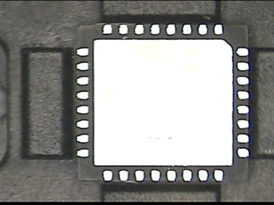
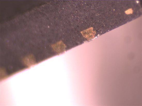
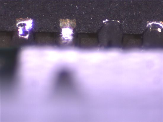
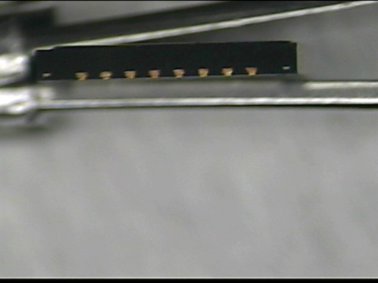
Please see attached photos of TI QFN P/N TPS62110.  Is it typical for this package to show the conditions we are seeing on some of the parts we have been receiving?  Concern number one, exposed copper seen on the side view photos and , plating underneath the part not reaching  to the edge of the package and inconsistent.  These conditions are causing a lot of rework in our factory and we have data that shows it is potentially causing noise inducing failures for us during Environmental Stress Screening (ESS).  We have been able to reflow parts and get the CCA to pass ESS test upon reflow.  Our concern is that we are not getting consistent or sufficient solder reflow because of these 2 conditions. 


Is there any way the plating can be enhanced to 1) consistently reach the edge of the package underneath and 2) eliminate the exposed copper?  Either by TI or a 3rd party we could consider.  Also, I assume this is a known condition to TI and considered acceptable or are we seeing something that may be attributed to how the parts are being stored, in particular, the exposed copper?  I’d appreciate your feedback.


  • I will ensure that someone from packaging reviews and comments on your question.

  • Rick,


    The exposed copper on the ends on the end of the leads is typical of most of our leaded packages including QFN’s.   The copper color is more pronounced on the QFN due to the size of the lead tip itself in relation to the package size.  The exposed lead tip has a long history starting with our PDIP and SOIC packages. The solder joint itself gets its strength from the wetting angle from the backside of the lead and not the lead foot end so wetability of the lead end doesn’t directly contribute to the strength of the joint.     Due to the lack of lead visibility, except the lead tips,  inspection of solder joint on a QFN is harder. 


    Generally speaking you can achieve better fillet results on lead tips by:


    You can see specific recommendation on how to use QFN’s and inspection methods and other facts by reviewing our application note on QFN’s recommendations at   http://focus.ti.com/lit/an/slua271a/slua271a.pdf

    High Activity Flux with Nitrogen

    Optimized reflow profile typically straight ramp to increase flux life during critical melting stage

    Using a Type 3 Solder Paste with at least 50% by volume of flux

    Adding pressure during placement to increase the contact height of solder on side of part but be cautious not to cause shorting.

    Increasing the volume of paste printed by modifying the stencil design.  Note that nickel buildup stencils will give the best solder paste printing results.