This thread has been locked.

If you have a related question, please click the "Ask a related question" button in the top right corner. The newly created question will be automatically linked to this question.

UCC21225A: Output Bias

Part Number: UCC21225A

Hi,

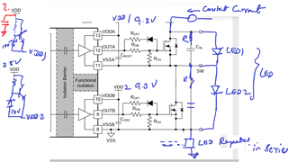
We are using this isolated driver (UCC21225A) in shunt pwm dimming for led string. LED's are driven by constant current source Representative schematics attached

1) Here the series regulator never get reverse biased , since vdd always higher than MID point voltage  (clamp by  LED parallel with dimming mosfet), Series regulator  always supply energy to boot cap.

  • Does the general rule of thump of Cinput= 10x CBoot apply here?
  • Do we even need a capacitor at the collector terminal (Cinput) of  series regulator transistor?

2) In the datasheet, he output pwm drive has an absolute maximum rating of -0.3v . If it exceeds (Negative going Spike< -0.3v) what is the failure mode,

  • Does the device latch to a certain state or will it get damaged? 

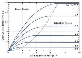
3) Can you think about a failure mechanism involving this chip , where this chip can take mosfet (high side or low side) out of saturation region to linear region and increasing its power dissipation?


Jacob

/resized-image/__size/320x240/__key/communityserver-discussions-components-files/196/led-question2.png

  • Hi Jacob,

    Are you trying to drive LED's directly? If so, I would recommended looking for an LED driver. It looks like you are driving FET's in your design? From the looks of it, it does not seem like you will require a bootstrap supply for your design. Cin just has to be big enough to handle whatever the Bus voltage will be and is different from Cboot. 

    I am not sure what you are referring to by out pwm drive. Can you please elaborate on that? Can you also share a schematic for your design? I would be glad to assist with that.

    Regards,

    Akshat

  • Akshat,

    Please review the question and attachment one more time, I made some edits and corrected couple of typos

    Jacob

  • Hi Jacob,

    1) Does the general rule of thump of Cinput= 10x CBoot apply here?

    The driver will drive the capacitors to charge and discharge the FET. The Cin is after FET for the LED so there is no general rule of thumb here. Cin has no connection with Cboot. I believe Cin's value needs to be determined from the FET or the LED. You can learn more about the bootstrap capacitor here.

    2) Do we even need a capacitor at the collector terminal (Cinput) of  series regulator transistor?

    The driver already has decoupling capacitors for the power supply pin. How you design the regulator circuit is up to you.

    3) In the datasheet, the output pwm drive has an absolute maximum rating of -0.3v . If it exceeds (Negative going Spike< -0.3v) what is the failure mode?

    Like I mentioned previously, I am not sure what exactly you mean by PWM drive. It sounds like you are referring to the output of the gate driver? If so, then no there is no latching to  any state for this device. if the voltage goes down to 0V it shouldn't be a problem. However, if it goes much lower than that, it can damage the driver.

    4) Can you think about a failure mechanism involving this chip , where this chip can take MOSFET(high side or low side) out of saturation region to linear region and increasing its power dissipation?

    Looking at the IV curve for a MOSFET, the different regions is only controlled by what the Vds is. This value is determined by the rest of the power circuitry. The gate driver only affects the Vgs voltage. So the driver will not affect moving from saturation to linear regions of operation. 

    Regards,

    Akshat

  • 1) Does the general rule of thump of Cinput= 10x CBoot apply here?

    The driver will drive the capacitors to charge and discharge the FET. The Cin is after FET for the LED so there is no general rule of thumb here. Cin has no connection with Cboot. I believe Cin's value needs to be determined from the FET or the LED. You can learn more about the bootstrap capacitor here.

    Akshat,

    Looks like thers is confusion over the term "Cinput". By Cinput what i meant was the Cvdd in the T.I application note

    Thanks for your hlep

    /resized-image/__size/320x240/__key/communityserver-discussions-components-files/196/pastedimage1665182227306v1.png

  • Hi Jacob,

    Yes, Cvdd should be 10xCboot or higher.

    Regards,

    Akshat