Other Parts Discussed in Thread: BQSTUDIO
Due to certain reason, I need to develop a sw & fw to upgrade GG setting without using EV2300 + Battery Management Studio.
I've develop a sw & fw to update few value in data flash.
The data flash address is referring to BQ40Z50-R4 Technical Reference Manual (the BQ is using R4 firmware).
The following table are the changes needed:
|
Data flash value |
GSI06 |
GSI07 |
|
Settings->Configuration->Balancing Configuration |
001b |
005f |
|
Advanced Charge Algorithm->Cell Balancing Config->Voltage Cell Balance Window |
10mV |
25mV |
|
Advanced Charge Algorithm->Cell Balancing Config->Voltage Cell Balance Min |
10mV |
25mV |
|
Advanced Charge Algorithm->Cell Balancing Config->Voltage Cell Balance Interval |
5Sec |
20Sec |
|
SBS Configuration->Data->Manufacturer Name |
GSI06 |
GSI07 |
|
Gas Gaugingà->IT Cfg->Design Resistance |
96 |
16 |
|
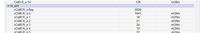
Ra Table->R_a0->Cell0 R_a 0 |
1841 |
17 |
|
Ra Table->R_a1->Cell1 R_a 0 |
1841 |
17 |
|
Ra Table->R_a2->Cell2 R_a 0 |
1841 |
17 |
|
Ra Table->R_a3àCell3 R_a 0 |
1841 |
17 |
|
Ra Table->R_a0x->xCell0 R_a 0 |
1841 |
17 |
|
Ra Table->R_a1x->xCell1 R_a 0 |
1841 |
17 |
|
Ra Table->R_a2x->xCell2 R_a 0 |
1841 |
17 |
|
Ra Table->R_a3x->xCell3 R_a 0 |
1841 |
17 |
After running the sw & fw, I found that all data have been successful updated except xCell0 R_a 0, xCell1 R_a 0, xCell2 R_a 0 and xCell3 R_a 0.
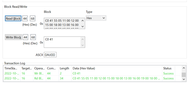
I'm sure that the sw & fw has successful write the value into address 0x41C2 (xCell0 R_a 0), 0x41E2 (xCell1 R_a 0), 0x4202 (xCell2 R_a 0) and 0x4222 (xCell3 R_a 0).
I have another sw & fw which is able to read data flash value from BQ and i found that address 0x41C2 (xCell0 R_a 0) has been updated to 0x11 (17).
During the verification, I found that 0x41C0 (xCell0 R_a flag) also not same with what shown on Battery Management Studio.
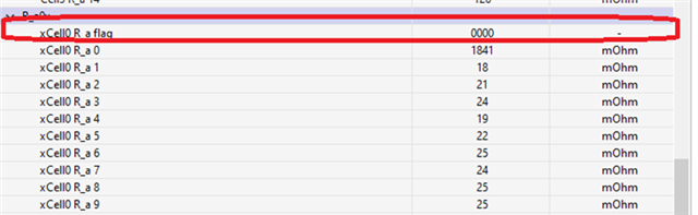
I would like to know why the value direct read from data flash is not tally with what shown on Battery Management Studio and is there any solution?