This thread has been locked.
If you have a related question, please click the "Ask a related question" button in the top right corner. The newly created question will be automatically linked to this question.
Hi TI
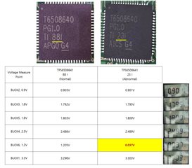
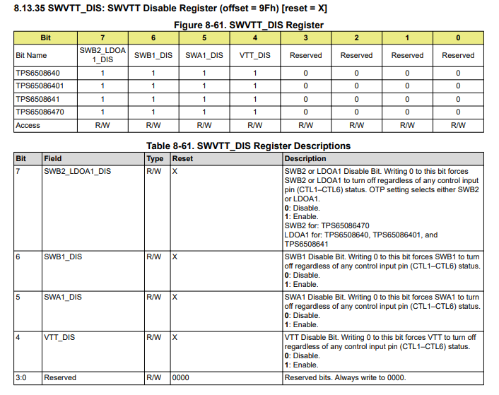
I am using TPS6508640, but there is a problem that BUCK6 1.2V is not output.
occurred in large numbers
Circuit, S/W abnormality, X-RAY inspection, but no problem
Finally, Laser Marking was checked.
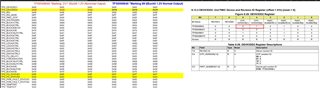
In 88 I, 1.2V is normally output, but
23 I output only 0.037V
Swap test of 88 I and 23 I was performed on a normal board
There was no output of 1.2V only at 23 I
I want to know why
Hello,
Thank you for reaching out via E2E and sharing the testing you have already conducted to look into this observation of BUCK6 not turning on.
Can you please help to provide some additional information to assist in the debug.
Finally can you clarify the results of the swap test. Did the 88 I version IC function correctly when you swapped it onto the board where you originally observed buck6 output = 0.037V?
Regards,
Garrett
Hello Garrett
Answer your inquiries
1. Can you provide a schematic of your board?
- Please check the attached "Circuit.pdf"
2. Can you provide two register logs, one from a board with buck6 correctly outputting 1.2V and one where you are observing buck6 output only 0.037V?
- Please check the attached "TPS6508340_register_log.txt"
3. When you perform this test is there a load connected to buck6? If so what is said load?
- The load is being checked. I will reply back as soon as it is confirmed.
4. Finally can you clarify the results of the swap test. Did the 88 I version IC function correctly when you swapped it onto the board where you
originally observed buck6 output = 0.037V?
- Yes, the 88 i version IC normal operating
Buck 6 1.2V OK ================================================= ==== ATTiny DTU Ver: V01.12 11:30:09 ==== ================================================= INFO : OTP [95], [95] INFO : Power falling [28][28] INFO : I2C Connect Device ID is 0x0 ========================= INFO : TPS_SWVTT_DIS is 0x70 INFO : TPS_SWVTT_DIS is 0x70 INFO : TPS_I2C_RAIL_EN1 is 0x80 INFO : TPS_I2C_RAIL_EN2_GPOCTRL is 0x01 INFO : TPS_PG_STATUS1 is 0x9f INFO : TPS_PG_STATUS2 is 0x26 INFO : TPS_PWR_FAULT_STATUS1 is 0x00 INFO : TPS_PWR_FAULT_STATUS2 is 0x00 ========================= INFO : I2C IRQ State is 0 INFO : I2C BUCK Read Data 0xe8 0x64 0x70 0xa8 0x70 0xa0 INFO : Buck 3 Setting value is 0x70 INFO : Buck 4 Setting value is 0xA8 INFO : Buck 6 Setting value is 0xA0 INFO : Buck 5 Setting value is 0x70 INFO : Buck1 0xE8 0xE8 INFO : Buck2 0x64 0x64 INFO : Buck3 0x70 0x70 INFO : Buck4 0xA8 0xA8 INFO : Buck5 0x70 0x70 INFO : Buck6 0xA0 0xA0 INFO : TPS650 Set ok Buck 6 1.2V Fail(0.037V) ================================================= ==== ATTiny DTU Ver: V01.13 14:38:15 ==== ================================================= INFO : OTP [95], [95] INFO : Power falling [24][24] INFO : I2C Connect Device ID is 0x0 ========================= INFO : TPS_SWVTT_DIS is 0xf0 INFO : TPS_SWVTT_DIS is 0x70 INFO : TPS_I2C_RAIL_EN1 is 0x80 INFO : TPS_I2C_RAIL_EN2_GPOCTRL is 0x01 INFO : TPS_PG_STATUS1 is 0x00 INFO : TPS_PG_STATUS2 is 0x20 INFO : TPS_PWR_FAULT_STATUS1 is 0x00 INFO : TPS_PWR_FAULT_STATUS2 is 0x00 ========================= INFO : I2C IRQ State is 0 INFO : I2C BUCK Read Data 0xe8 0x64 0x40 0x28 0x70 0xbe INFO : Buck 3 Setting value is 0x70 INFO : Buck 4 Setting value is 0xA8 INFO : Buck 5 Setting value is 0x70 INFO : Buck 6 Setting value is 0xA0 INFO : Buck1 0xE8 0xE8 INFO : Buck2 0x64 0x64 INFO : Buck3 0x70 0x70 INFO : Buck4 0xA8 0xA8 INFO : Buck5 0x70 0x70 INFO : Buck6 0xA0 0xA0 INFO : TPS650 Set ok
Thank you
Hi,
Garrett is out of office. Please expect a reply early next week.
Thanks,
Daniel W
Hello,
Thank you for providing your register log and schematic. Please see my comments below.
First, taking a look at your schematic I have a couple questions.
Then looking at the register log I have the following comments. In general can you provide a full register log(in the log you attached various registers are not provided).
The load is being checked. I will reply back as soon as it is confirmed.
Thank you for looking into the load that is attached. For debug I recommend disconnecting BUCK6 output from its load to check if the observation of no output voltage is load related.
Regards,
Garrett
Hello Garrrett
Answer your inquiries
1. Can you confirm if resistor R74 is or is not populated on your board? If so what is its value?
What is the meaning of the blue shaded area over the input capacitors on BUCK6 (C73 and C74)?
- It is uninserted. It is added in preparation for future circuit changes, and the corresponding part is the same as the EVM Circuit.
2. What is the meaning of the blue shaded area over the input capacitors on BUCK6 (C73 and C74)?
- This was added to match the TPS6508640 EVM Circuit.
3. 1, 2 Check Result : It was confirmed that the Buck6 Circuit is the same as the EVM Circuit provided by TI
4. The result of reading all resistors is as follows
- Check result : TPS_DEVICEID2 seems to be different please check the attached file
TPS6508640_Register_check(221011).xlsx
- "Marking 23 I" where Buck6 1.2V is abnormal output and "Marking 88 I" where Buck6 1.2V is normal output are different
It is identified as a register that cannot be controlled by Infocube (Read only).
5. Thank you for looking into the load that is attached. For debug I recommend disconnecting BUCK6 output from its load to check if the observation of no output voltage is load related.
- As requested, disconnect the BUCK6 output from the load and check if there is no output voltage to see if it is related to the load.
By the way, please explain why 1.2V" is normally output in Marking "88 I" regardless of the load.
Was there a change in the circuit after Marking "88 I" on FEB?
There was never a 1.2V non-output in the Marking "88 I" I used so far.
Thank you
Hello,
Thank you for answering my various questions.
1/2) Based off your responses I agree that everything in your schematic looks good.
4) I am working with our internal resources to see if the different markings on the package "88 I" vs "23 I" is related to the difference in OTP version observed on the newest register log.
Looking further into your register settings I see some voltages, specifically BUCK3 and BUCK4, are different that the default set by OTP memory on the TPS6508640. Have you attempted to make adjustments to the OTP memory or are you changing the regulation voltage after power up?
As requested, disconnect the BUCK6 output from the load and check if there is no output voltage to see if it is related to the load.
Do you have results from testing the "23 I" device with no load? Do you observe the expected 1.2V with no load attached to BUCK6?
By the way, please explain why 1.2V" is normally output in Marking "88 I" regardless of the load.
We will need to determine potential differences with the device marked "23 I" to answer why it does not work with your load if the observation is determined to be related to loading of BUCK6.
Regards,
Garrett
Hello Garrrett
Answer your inquiries
1. Looking further into your register settings I see some voltages, specifically BUCK3 and BUCK4, are different that the default set by OTP memory on the TPS6508640.
Have you attempted to make adjustments to the OTP memory or are you changing the regulation voltage after power up?
- We do not modify the OTP memory, but modify the values of BUCK3(0X70) / BUCK4(0XA8) / BUCK6(0XA0) by referring to the Register Map of the DataSheet to set the voltage we want to use.
TPS6508640_Register_check(221012).xlsx
2. JAEMOON GOO said:
As requested, disconnect the BUCK6 output from the load and check if there is no output voltage to see if it is related to the load.
Do you have results from testing the "23 I" device with no load? Do you observe the expected 1.2V with no load attached to BUCK6?
- The board to be tested is a board for delivery to the customer. To remove the load connected to BUCK6, it is impossible to remove the associated memory, diode, etc.
TPS6508640 "Marking 88 I" inspected and delivered more than 1,000 pieces to the customer, but this has never happened.
I got the EVM Board 2EA from TI today.
I will test by attaching "Marking "23 I" and "Marking 88 I" to the EVM Board.
"Marking 23 I" is in stock over 50EA There is an issue with the delivery date of the customer. If you can provide us with "Marking 88 I" for free, please provide it.
Otherwise, please solve this problem by the next week at the latest.
Thank you
Hello,
Thank you for answering my inquiries.
Upon doing further research and testing I agree with you that I do not think the issue is load related. Could you please try to test one register change to see if it fixes the output on BUCK6. Please try changing SWVTT_DIS (register address 9F hex) from your setting of 70 hex back to the default F0 hex. I have included the relevant Register Map section below.
Let me know if this change allows you to observe BUCK6 = 1.2V on "23 I' marked device.
Regards,
Garrett
Hello Garret Kreger
Upon doing further research and testing I agree with you that I do not think the issue is load related.
Could you please try to test one register change to see if it fixes the output on BUCK6. Please try changing SWVTT_DIS (register address 9F hex) from your setting of 70 hex back to the default F0 hex.
I have included the relevant Register Map section below.
Let me know if this change allows you to observe BUCK6 = 1.2V on "23 I' marked device
Reply : BUCK6 = 1.2V output at "Marking 23 I" as a result of the resistor change test
As a result of the resistor change test in "Marking 26 I" on the board for delivery to another customer owned by Infocube, BUCK6 = 1.2V output
Question
I have additional questions
1. Is there any problem when applying the same Resister change test in "Marking 88 I"?
(There should not be any problems because the test is performed on the board for delivery to the customer)
If you answer that there is no problem, I will test it.
2. If there is a problem, what difference between "Marking 23 I" and "Marking 88 I" causes the problem?
Thank you
Hello Garret Kreger
If you have additional questions within Infocube, please contact us once more.
Please try changing SWVTT_DIS (register address 9F hex) from your setting of 70 hex back to the default F0 hex.
-> As described above, when SWVTT_DIS Register was modified to 0xF0, Buck6 output 1.2V.
As a result of additionally checking the datasheet, looking at the revision history, there is a related part (LDOA1) of SWVTT_DIS Register.
Comparing the PMIC Functional Block Diagram of Rev C with the PMIC Functional Block Diagram of Rev D, it was confirmed that the presence of the indicated line in the figure below has changed.
In Rev C (Marking 88 I), the output of Buck6 is displayed regardless of Bit 7 (SWB2_LDOA1_DIS) of SWVTT_DIS.
In Rev D (Marking 23 I, 26 I), Bit 7 (SWB2_LDOA1_DIS) of SWVTT_DIS must be enabled to produce Buck6 output.
I wonder if the reason has anything to do with the presence or absence of the indicated line in the PMIC Functional Block Diagram.
If it doesn't matter, I'd like you to explain why it's different.
Thank you
Hello Jaemoon Goo,
Great to hear that the register change fixed the observed issue on the devices with "23 I" marking. Please see my comments below in regards to your questions.
1) No, there is no issue with making the same register change to devices marked "88 I". The register change just enables the LDOA1 rail. As long as LDOA1 rail being on is not an issue in the end system there should be no problem.
2) The indicated line in the PMIC functional block diagram has nothing to do with the matter. That datasheet update was simply a cosmetic update to the figure. The difference between the marking "88 I" device and the marking "23 I" device is a slight difference in the sequencing of the rails set by OTP memory. On the "23 I" device BUCK6 turn on is gated by LDOA1 being ON. Therefore, when LDOA1 was disabled via SWVTT_DIS register BUCK6 remains off. In the older marking "88 I" device the opposite is true. LDOA1 turn on is gated by BUCK6 being ON. This is why BUCK6 turn on is not affected by LDOA1 being disabled on devices marked "88 I."
Let me know if you have any further questions.
Best Regards,
Garrett