Hi
According to the user’ s guide of BQ24800 EVM
2
The IC should be placed close to the switching MOSFET’s gate pins and keep the gate drive signal traces short for a clean MOSFET drive.
The IC can be placed on the other side of the PCB from the switching MOSFETs
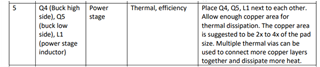
The recommendation will turn out to be the following brief stack illustration
Take 4-layer as an example

It is beneficial to the design of small form factors and layout simplified
That is highly different from the EVM shown.
We have no idea whether this implementation is feasible or not
Could you please comment on our intended layout design?
In addition, the width of the trace is current-carried depend. How do we estimate the track route to the MOSFET gate?
Thanks
Regards
Ben