


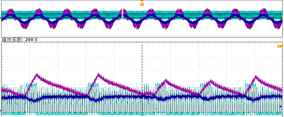
Hello, the main circuit on my side is changed according to the circuit topology of UCD3138PFCEVM-026, the EMI filter circuit is removed, and the sampling ratio in the sampling circuit is changed, and the controller is changed from UCD3138 to DSP28335 for PFC dual-loop PI control. At present, single-phase Boost PFC is tested with parameters: 20VAC input during low-voltage test, set output 50VDC, load 100 ohms, switching frequency of 100kHz dual-loop program. Sampling ratio: The ratio of input voltage hardware is 5.1k/605.1k, the sampling ratio of inductor current is 499/1200, and the sampling ratio of output voltage is 2.4k/402.4k. Procedure: Set two PWMs, where PWM1 period is 100kHz, trigger the ADC to sample (all variables take a point in a switching cycle), the ADC triggers the interrupt, and the interrupt function runs the two-ring control program. During the test, the PWM duty cycle is either 0 or the maximum value set for the current loop, where, as shown in the figure, purple is the input current, light blue is the drive signal waveform, and dark blue is the input voltage waveform. What might be the problem?
void main()
{

    InitSysCtrl();
    MemCopy(&RamfuncsLoadStart, &RamfuncsLoadEnd, &RamfuncsRunStart);
    InitFlash();

    EALLOW;
    SysCtrlRegs.HISPCP.all = ADC_MODCLK;

    EDIS;
    DINT;

    InitEPwm1Gpio();
    InitEPwm2Gpio();

    InitPieCtrl();
    IER = 0x0000;
    IFR = 0x0000;
    InitPieVectTable();

    EALLOW;
    PieVectTable.ADCINT = &adc_isr;
    EDIS;
    InitAdc();
    PieCtrlRegs.PIEIER1.bit.INTx6 = 1;
    IER |= M_INT1; // Enable CPU Interrupt 1
    EINT;// Enable Global interrupt INTM
    ERTM;// Enable Global realtime interrupt DBGM

    EALLOW;
    SysCtrlRegs.PCLKCR0.bit.TBCLKSYNC = 0;
    SysCtrlRegs.PCLKCR1.bit.EPWM1ENCLK = 1;
    SysCtrlRegs.PCLKCR1.bit.EPWM2ENCLK = 1;
    EDIS;

    InitADC();
    InitEPwm1Example();
    InitEPwm2Example();
    Disable_boost_PWM();

    EALLOW;
    SysCtrlRegs.PCLKCR0.bit.TBCLKSYNC = 1;
    EDIS;

    for (;;)
    {

    }
}

void InitEPwm1Example()
{

   EPwm1Regs.TBPRD = 750;
   EPwm1Regs.TBPHS.half.TBPHS = 0x00;
   EPwm1Regs.TBCTR = 0x0000;
   EPwm1Regs.TBCTL.bit.CTRMODE = TB_COUNT_UPDOWN;
   EPwm1Regs.TBCTL.bit.PHSEN = TB_DISABLE;
   EPwm1Regs.TBCTL.bit.SYNCOSEL = TB_CTR_ZERO;

   EPwm1Regs.TBCTL.bit.HSPCLKDIV =0x00;
   EPwm1Regs.TBCTL.bit.CLKDIV = 0x00;

   EPwm1Regs.DBCTL.bit.IN_MODE =0;
   EPwm1Regs.DBCTL.bit.POLSEL =2;
   EPwm1Regs.DBCTL.bit.OUT_MODE =3;

   EPwm1Regs.CMPCTL.bit.SHDWAMODE = CC_CTR_ZERO;
   EPwm1Regs.CMPCTL.bit.LOADAMODE = CC_CTR_ZERO;

   EPwm1Regs.CMPA.half.CMPA = 750;

   EPwm1Regs.AQCTLA.bit.ZRO = AQ_SET;
   EPwm1Regs.AQCTLA.bit.CAU = AQ_CLEAR;

   EALLOW;
   // What do we want the TZ1 and TZ2 to do?
   EPwm1Regs.TZCTL.bit.TZA = TZ_FORCE_LO;
   EPwm1Regs.TZCTL.bit.TZB = TZ_FORCE_LO;

   // Enable TZ interrupt
   EPwm1Regs.TZEINT.bit.OST = 1;
   EDIS;
//(Q:用于触发ADC转换)
   EPwm1Regs.ETSEL.bit.SOCAEN = 1;
   EPwm1Regs.ETSEL.bit.SOCASEL = 2;
   EPwm1Regs.ETPS.bit.SOCAPRD = 1;

}

void InitEPwm2Example()
{

   EPwm2Regs.TBPRD = 750;
   EPwm2Regs.TBPHS.half.TBPHS = 0x00;
   EPwm2Regs.TBCTR = 0x0000;

   EPwm2Regs.TBCTL.bit.CTRMODE = TB_COUNT_UPDOWN     ;
   EPwm2Regs.TBCTL.bit.PHSEN = TB_DISABLE;
   EPwm2Regs.TBCTL.bit.SYNCOSEL = TB_CTR_ZERO;

   EPwm2Regs.TBCTL.bit.HSPCLKDIV =0x00;
   EPwm2Regs.TBCTL.bit.CLKDIV = 0x00;

   EPwm2Regs.DBCTL.bit.IN_MODE =0;
   EPwm2Regs.DBCTL.bit.POLSEL =2;
   EPwm2Regs.DBCTL.bit.OUT_MODE =3;

   EPwm2Regs.CMPCTL.bit.SHDWAMODE = CC_CTR_ZERO;
   EPwm2Regs.CMPCTL.bit.LOADAMODE = CC_CTR_ZERO;

   EPwm2Regs.CMPA.half.CMPA = GD_EPWM1_CAMPA1;
   EPwm2Regs.AQCTLA.bit.CAD  = AQ_SET;
   EPwm2Regs.AQCTLA.bit.CAU = AQ_CLEAR;

   EALLOW;
   // What do we want the TZ1 and TZ2 to do?
   EPwm2Regs.TZCTL.bit.TZA = TZ_FORCE_LO;
   EPwm2Regs.TZCTL.bit.TZB = TZ_FORCE_LO;
   // Enable TZ interrupt
   EPwm2Regs.TZEINT.bit.OST = 1;
   EDIS;

}

void InitADC()
{
    AdcRegs.ADCTRL1.bit.CPS = 1;
    AdcRegs.ADCTRL3.bit.ADCCLKPS = ADC_CKPS;

    AdcRegs.ADCTRL1.bit.ACQ_PS = ADC_SHCLK;
    AdcRegs.ADCTRL1.bit.SEQ_CASC = 1;
    AdcRegs.ADCTRL1.bit.SEQ_OVRD = 0;
    AdcRegs.ADCTRL1.bit.CONT_RUN = 0;
    AdcRegs.ADCTRL3.bit.SMODE_SEL = 0;
    AdcRegs.ADCMAXCONV.bit.MAX_CONV1 = 0x4;
    AdcRegs.ADCCHSELSEQ1.bit.CONV00=0x02;
    AdcRegs.ADCCHSELSEQ1.bit.CONV01=0x03;
    AdcRegs.ADCCHSELSEQ1.bit.CONV02=0x04;
    AdcRegs.ADCCHSELSEQ1.bit.CONV03=0x05;

    AdcRegs.ADCTRL2.bit.EPWM_SOCA_SEQ1 = 1;
    AdcRegs.ADCTRL2.bit.INT_ENA_SEQ1 = 1;
    AdcRegs.ADCTRL2.bit.INT_MOD_SEQ1 = 0;
}

interrupt void  adc_isr()
{
    while(AdcRegs.ADCST.bit.INT_SEQ1==0) {}

    Value_Detection();

    Enable_boost_PWM();

    rectify_vac();

    handle_voltage_loop();

    calculate_current_target_shunt();

    current_PIcontrol();

    GD_EPWM1_CAMPA1=(int) (750.0 * Current_Output1);
    EPwm2Regs.CMPA.half.CMPA = GD_EPWM1_CAMPA1;

    EPwm1Regs.ETCLR.bit.SOCA = 1;
    AdcRegs.ADCTRL2.bit.RST_SEQ1 = 1;         // Reset SEQ1
    PieCtrlRegs.PIEACK.all = PIEACK_GROUP1;   // Acknowledge interrupt to PIE
    AdcRegs.ADCST.bit.INT_SEQ1_CLR=1;
    return;
}


void Value_Detection()
{
    SampleTable0 = ( (AdcRegs.ADCRESULT0)>>4);  //Vl

    SampleTable1 = ( (AdcRegs.ADCRESULT1)>>4);  //VN

    SampleTable2 = ( (AdcRegs.ADCRESULT2)>>4);  //IL

    SampleTable3 = ( (AdcRegs.ADCRESULT3)>>4);  //VO

    value_temp1 = SampleTable0 *(2017.0/23205.0) ;
    Sample_vl   = value_temp1 ;

    value_temp2 = SampleTable1 *(2017.0/23205.0) ;
    Sample_vn   = value_temp2 ;

    value_temp3 = SampleTable2 *(80.0/45409.0);
    Sample_il   = value_temp3 ;

    value_temp4 = SampleTable3 *(503.0/4095.0);
    Sample_vo   = value_temp4 ;
}

void rectify_vac ()
{
    if (Sample_vl > Sample_vn )
    {
        Vin_raw = Sample_vl - Sample_vn;

        Vin_positive = 1.0;
    }
        else //cycle for neutral
        {
        Vin_raw = Sample_vn - Sample_vl;

        Vin_positive = 0.0;
        }

      Vin_sum = Vin_raw + Vin_sum - (Vin_sum * 0.25);
      Vin_filtered = Vin_sum * 0.25;

      Vin_squared = (Vin_filtered * Vin_filtered);
}

void handle_voltage_loop()
{

    Current_i_target_average =  proportional_integral(50.0 - Sample_vo);
}


float proportional_integral(float voltage_Error)
{
    Voltage_Error = voltage_Error;

    Voltage_Output1=0.01 *(Voltage_Error-Voltage_Error11) + 1.0 * Voltage_Error ;

    Voltage_Output = Voltage_Output + Voltage_Output1 ;

    if ( Voltage_Output > 1.4 )
    {
        Voltage_Output = 1.4;
    }

    else if ( Voltage_Output <= 0.0 )
        {
        Voltage_Output =0.0;
        }

    Voltage_Error11 = Voltage_Error ;

    return Voltage_Output;
}

void calculate_current_target_shunt()
{
    Current_i_target_sensed = (( Current_i_target_average * Vin_filtered )/20.0);

    if(Current_i_target_sensed > 2.0)
    {
    Current_i_target_sensed = 2.0  ;
    }
    else if(Current_i_target_sensed < 0.0)
    {
        Current_i_target_sensed = 0.0  ;
    }
}

void current_PIcontrol()
{
    Current_Error1 = Current_i_target_sensed - Sample_il ;

    Current_Output11 = 1.5 *( Current_Error1-Current_Error11) + 600.0 * Current_Error1;//KP=1.5,KI=600

    Current_Output1 = Current_Output1 + Current_Output11 ;
    if ( Current_Output1 > 0.9 )
    {
        Current_Output1=0.9 ;
    }
    else if( Current_Output1 <=0.0 )
    {
        Current_Output1=0.0 ;
    }
    Current_Error11 = Current_Error1 ;
}

void Disable_boost_PWM()
{
    EALLOW;
    GpioCtrlRegs.GPAMUX1.bit.GPIO2 = 0;
    GpioCtrlRegs.GPADIR.bit.GPIO2  = 1;
    GpioCtrlRegs.GPAMUX1.bit.GPIO3 = 0;
    GpioCtrlRegs.GPADIR.bit.GPIO3  = 1;
    EDIS;
    GpioDataRegs.GPACLEAR.bit.GPIO2=1;
    GpioDataRegs.GPACLEAR.bit.GPIO3=1;
}

void Enable_boost_PWM()
{
    EALLOW;
    GpioCtrlRegs.GPAMUX1.bit.GPIO2 = 1;
    GpioCtrlRegs.GPADIR.bit.GPIO2  = 1;
    GpioCtrlRegs.GPAMUX1.bit.GPIO3 = 1;
    GpioCtrlRegs.GPADIR.bit.GPIO3  = 1;
    EDIS;
}
