This thread has been locked.

If you have a related question, please click the "Ask a related question" button in the top right corner. The newly created question will be automatically linked to this question.

LM5118-Q1: LM5118-Q1 stability issues

Part Number: LM5118-Q1
Other Parts Discussed in Thread: LM5118, LMP8646

Hi 

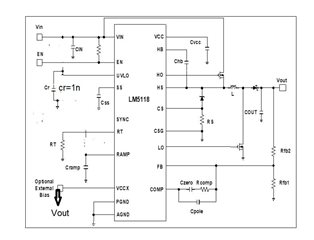
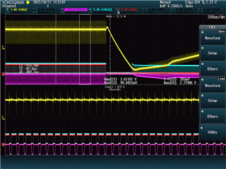
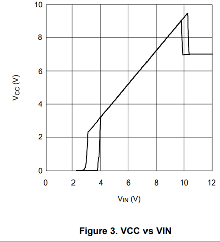
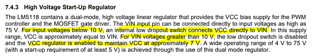
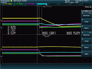
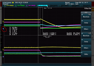
I am using LM5118 to design power supply of 5V,3A . The regulator works fine with buck operation. However, when the input voltages reaches close to 5V, it got stability issues and output is decreasing and stuck at approx. 2.5V. I am expected to work the regulator from 3.5 to 70V without any issues. Calculator sheet and excel attached below.  I have tied VCCX pin to output.                       5Vo 2.8Ao 10uH IPG5 B-Sample 5VAux LM5118 calculator_Ti.xlsm

  • With 2.7A, the regulator fails to regulate <5.1V, With 2.5A, the regulator fails to regulate <4.4V

  • Hello, 

    Thanks for reaching out. Can you please share the schematics of your circuit? Would it be possible to share a scope plot with the CS pin, the FB pin and the gates of the two MOSFETs? We're looking forward hearing back from you soon.

    Kind regards, 
    EM

  • Hello 

    Thanks for the reply. Please find the attached.

    Thanks

    Sibilgate_driver.pdf

  • Channel3-CS, Channel 4 and 5- Gate, channel 1- output

  • Hello, 

    Thanks for your response, we are currently looking into this and will come back to you as soon as possible. 

    Kind regards,

    EM 

  • Thank you. I think it may be something to do with Rds(on) of the MOSFET. I can see that MOSFET is really getting hot at 4.5V(so possibly large voltage drop) and the boost gate signals are disappearing. I am just wondering how IC is detecting this? Is it via sense resistor drop?

  • Hi Sibildas,

    I think you might be right here. What is the gate plateau voltage of your MOSFETs (alternatively you can also share the par number)? For a Vin up to 10V, the VCC is following the Vin and the the MOSFET is driven with a voltage equal to the Vin (see Fig. 3): 

    See this section for the description:

    If your MOSFET is getting hot, it might mean that it is working in linear region and therefore it is not being turned on properly. We're looking forward to hearing from you. 

    Kind regards,
    EM

  • Thanks for the response. The MOSFET that I am using is IPG20N10S4L-35.  Gate plateau voltage is 3.5V( under the test condition of (VDD=80 V, ID=20 A, VGS=0 to 10 V)

  • Hello Sibildas, 

    Can you please probe the VCC pin, SS  and the UVLO too to check how they look like?

    Kind regards,

    EM 

  • Please find below:

    1- output

    2-ss

    3-UVLO

    4-VCC

  • Hello Sibildas, 

    Thanks for sharing the scope shot. We are now looking into this and will come back as soon as possible. 

    Kind regards,
    EM

  • Hello, 

    With the chosen MOSFET this design will not work down to 3.5 V of input voltage. In this case, a MOSFET with a lower plateau should be chosen (e.g. a logic level one). 

    Row 42 of the Excel file is the current limit margin, which should fall in the suggested range 5% to 20% otherwise the device might hit current limit during normal operation. Could you please try to decrease the sense resistor e.g. to 18mOhm and see if the issue is solved? 

    Kind regards,
    EM 

  • Hello

    Thanks for the response. I have already tried to decrease the current sensor to up to 12mOhm and it didn't worked. The device was tripped before reaching the 4.5V.

    I have tried a new MOSFET IPG20N10S4L22ATMA1 with lower RDS(ON) and lower plateau. The performance is better as the regulator is worked up to 4.2V before the MOSFET temperature goes beyond >130degC.  Then, the regulator boost signals are disappeared. 

    Thanks

    Sibil

  • Hello, 

    Thanks for sharing this with us. As we are looking into this, could you please share as well the layout of this board (if you are not using the EVM)? Is the saturation current of the inductor above the current limit threshold of the controller?  

    Kind regards,
    EM 

  • Yes, Saturation current would be OK. The inductor can take up to 16A.

    Please find below the layout. I dont know is it enough or you need more information. This supply is part of our board.

  • I have inductors and input capacitors on the other side of the 7 layer board. The below shows IC, diode, Mosfet(dual mosfet) and output diode

  • Hello Sibildas,

    If you reduce the output current, does the converter work properly with the new MOSFETs down to the voltage you expect it to work?

    If yes, I expect that the power dissipation in your MOSFET and diodes is too high. The power dissipation mostly happens through the board and you need metal areas to spread the heat on the board and into the air. Your layout seem to have little metal areas that can be used by the MOSFETs and diodes to dissipate. 

    Best regards,
    Brigitte

  • Yes, If I reduce the current by say 0.5A to 1A. Its works fine. 

    OK, With new MOSFET(LOW Rds on) the performance was better. So, will try to spread out the heat in next revision of PCB. 

    Can you please give me an explanation how the IC is managed to turn off the boost gate signals when the the drop across the MOSFET and diode is high.  Is it via sense resistor or error amplifier or something else?

  • Hi Sibildas,

    the device has a current limit implemented which is sensing through the current sense resistor.
    See also datasheet chapter 7.3.5 Current Limit for more details.

    To get a clearer picture on the power dissipation it would be good to measure the temperature of the MOSFETs during operation.
    Best is to us a thermal camera but also a temp. resistor/sensor connected to the MOSFET case can be used.

    Best regards,

     Stefan

  • Hi Stefan

    Thanks for the message. Then why decreasing current sensor value didn't helped me?  I have used a very big inductor (to check) to avoid the saturation of the inductor for higher currents

    Thanks

    Sibil

  • Hi Sibildas,

    decreasing the current sense resistor will reduce the voltage drop and loss on the current sense resistor but not change the loss on the FET.

    Best regards,

     Stefan

  • The current limit is sensed via current sensor resistor. I thought even if the MOSFET has more drop, the regulator will try to regulate the output voltage if I keep the current limit threshold higher?

  • Hi Sibildas,

    I am just trying to wrap up the full thread again from the beginning. To get the full picture and hopefully get to the solution.

    One initial point which might was missed is your statement: " I have tied VCCX pin to output."

    Please try to reproduce this measurement with disconnecting VCCX from the output (connect to GND instead would be good).
    Note: for this device the VCCX should only be connected to the output once the output voltage has completely ramped up.

    Please let me know if this changes the behavior you have seen with the boost mode.

    Next i had a look into the scope plot you have shared above with  1- output  2-ss 3-UVLO 4-VCC.

    Can you explain which condition this shows? This when going down with Vin and where the output voltage drops?
    Can you explain where the ground reference of all the signals is located - is this the marker at the left - is this for all 4 channels identical?


    Can please also try to replace the MOSFET with one which has a lower Miller Plateau / Gate Threshold.

    The gate signal is generated out of Vcc which is dependent on the input voltage, see: Figure 3. VCC vs VIN

    With an input voltage of 3.5V -> Vcc will be down to ~3 V.

    This is far below the level to open the MOSFET properly. I would at least suggest to be 1V above the Miller Plateau

    Thanks,

     Stefan

  • Note: as in interim test you can also try to supply Vcc from external with e.g. 7V and check if the system the works as expected.

    Best regards,

     Stefan

  • Hi Stefan 

    Thanks for the detailed response.

    You meant VCC or VCCX pin? I have already tried to supply VCCX externally with 6.5V supply and it doesn't helped. 

    Please try to reproduce this measurement with disconnecting VCCS from the output (connect to GND instead would be good).

    I think I already tried this and behavior was same. But, I will reconfirm and post here in case of any changes.

    Can you explain which condition this shows? This when going down with Vin and where the output voltage drops? Yes, You are right
    Can you explain where the ground reference of all the signals is located - is this the marker at the left - is this for all 4 channels identical? Yes, I have marked in the picture below.

    Can please also try to replace the MOSFET with one which has a lower Miller Plateau / Gate Threshold. I cant do this now because of my footprint. I have used the least available in the market with this footprint.

    The gate signal is generated out of Vcc which is dependent on the input voltage, see: Figure 3. VCC vs VIN

    With an input voltage of 3.5V -> Vcc will be down to ~3 V. I am loosing the output voltage when the input voltage is around 4.5V, that means VCC to 4V. My Plateau voltage of the MOSFET is 3V. Will this be OK?

    This is far below the level to open the MOSFET properly. I would at least suggest to be 1V above the Miller Plateau. OK, I will try to use better one in the next iteration of the PCB, if possible.

  • Hi Sibildas,

    sorry for the type - it should be VCCX.

    To the scope plot:

    As you can see UVLO will drop to 0V - I am not sure what is causing this as UVLO typically is generated out of VIN, but with UVLO the device will switch off.
    So please try to check in this, e.g. check if your supply is stable and able to provide the required current.

    Best regards,

     Stefan

  • I agree. not sure what is happening. I am using a 20A input voltage source. So, I believe my input is good. 

    I am not using UVLO to switch off. Just connected a10NF for the hiccup. 

  • Hi Sibildas,

    if the input is stable in then the other option would be an detected over current.

    This means that the current on the Current sense resistor reached the over current limit.

    Can you check this, e.g. probe the voltage on the current sense resistor

    Best regards, 

     Stefan

  • Hi Sibildas,

    it looks like that you are very close to the over current limit based in the scope plot.

    Can you try to reduce the current sense resistor to a lower level and check again.

    Best regards,

     Stefan

  • HI Stefan

    I did that. I have reduced the sense resistor to 12 from 24mohm. It didn't helped. The MOSFET got heat up to 140degC before the boost signal turned off.

    If you read through my messages above, its some what obvious that its something to do with the heating of the MOSFET(Rds. and drop). I am trying to understand how the large drop on the MOSFET cause boost signal to turned off?  I think it might be sense resistor drop is going above the limit. But how its happening when the drop across the MOSFET is increasing?

    Thanks

    Sibil

  • Hi Sibildas,

    have you already checked this:

    Can please also try to replace the MOSFET with one which has a lower Miller Plateau / Gate Threshold.

    The gate signal is generated out of Vcc which is dependent on the input voltage, see: Figure 3. VCC vs VIN

    With an input voltage of 3.5V -> Vcc will be down to ~3 V.

    This is far below the level to open the MOSFET properly. I would at least suggest to be 1V above the Miller Plateau

    Best regards,

     Stefan

  • Hi Stefan


    I cant change the MOSFET now because of my footprint(dual Mosfet package which I am using got 3V gate plateau, that only available in the market). I will change it in the next iteration of PCB. It will take some time. 

    So, the possible explanation is the higher Miller Plateau causing this issue? But, at 4.5Vin, the MOSFET should be ok.  Not sure, what's happening there.

    Thanks

    Sibil

  • Hi Sibildas,

    again - check figure 3 in the datasheet: with Vin of 4.5V you will get a Vcc of ~3.5V

    With 3.5V you are exactly at the Miller Plateau and your MOSFET will not fully open and produce a lot of loss.

    Best regards,

     Stefan

  • Hi Stefan

    Thank you. That explains the second MOSFET(Have Plateau of 3V compared with first one that got 3.5V) behaved better compared with the first one.

    Thanks for your time. 

    Regards

    Sibil

  • Hi Sibildas,

    thanks for the feedback.

    So, I will close this thread.

    Best regards,

     Stefan

  • Actually, I have tied my output to the VCCX, so  the below point is valid? I would expecting a constant supply at Vcc. 

    again - check figure 3 in the datasheet: with Vin of 4.5V you will get a Vcc of ~3.5V

  • Also, I have tried an external supply with constant supply of 5V

  • Hi Sibildas,

    can you also check with supplying Vcc of the LM5118 with 6V or 8V?

    Does it then work as expected?

    At which level you see here the MOSFET heating up?

    Best regards,

     Stefan

  • Hi Stefan 

    Thanks for the reply. I have supplied VCCX is with an external supply of 6.5V. The regulator worked only up to 4.3V (short duration).  Actually, my design requirement is regulator needs to work for the voltage up to 3.8V for the duration of 100ms. 9V is my normal input voltage. But, regulator should able to provide constant supply when there is a dip in the supply for the duration of 100ms.  So, all I am doing simulation dip in the input voltage. Up to 4.2-4.3V  its worked. But, for voltage less than that didn't worked. 

    The MOSFET temperature was normal when I was doing the dip in the input supply. I have applied a freezer spray as well to exclude the heating problem.

    Please note that I have also tried slowly reducing the voltage with freezer spray. The result was same. The regulator worked only up to 4.2-4.3V.

    Thanks

    Sibil

  • Hi Sibildas,

    I am not sure if I still the full and right picture.

    May you can summarize - esp. when the device stops working and the output is not stable or avaialbe and when the MOSFET gets hot.

    Please also - do not use VCCX for this tests - connecte VCCX to GND

    Supply Vcc from external with 6.5V.

    Are the MOSFET still getting hot when going down with Vin.

    If yes, please check the voltage level on the Gate signals?

    Thanks,

     Stefan

  • Hi Sibildas,

    I have not seen an update for the last 14 days, so I assume the questions are/or answered and the issue is solved.
    I close this thread now. If there is still something open reply and the thread will get open again.
    If you have any other question or of the thread gets locked, please open a new one.

    Clicking the Resolved Button also helps us to maintain this forum.

    Best regards,
    Stefan

  • Hello Team,

    We are using the LM5118 also , along with LMP8646 to limit current so that it behaves as a CC source. We will design the LM5118 for 54.6V with the current limit of 3A. So we expect the LM5118 to behave as CC mode during charging a battery from 42V to 54.6V.

    We found this in the LM5118 datasheet under current limiting "To further protect the external switches during prolonged overload conditions, an internal counter detects consecutive cycles of current limiting. If the counter detects 256 consecutive current limited PWM cycles, the LM5118 enters a low power dissipation hiccup mode. In the hiccup mode, the output drivers are disabled, the UVLO pin is momentarily pulled low, and the soft-start capacitor is discharged. The regulator is restarted with a normal soft-start sequence once the UVLO pin charges back to 1.23 V. The hiccup mode off-time can be programmed by an external capacitor connected from UVLO pin to ground. This hiccup cycle will repeat until the output overload condition is removed"

    So is this for peak current limiting at 54.6V,3A in our application? or the CC stage of the LM5118 when charging the battery where the voltage would vary between 42V to 54.6V but keeping 3A current limit

    Could you kindly clarify this 

    Thanks

  • Hello Bhanu,

    As I answered this in the other thread, I close this thread now.

    Best regards,
    Brigitte