This thread has been locked.

If you have a related question, please click the "Ask a related question" button in the top right corner. The newly created question will be automatically linked to this question.

TPS7A4701-EP: Output abnormal

Part Number: TPS7A4701-EP
Other Parts Discussed in Thread: TPS798-Q1

Hi Experts,

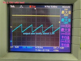
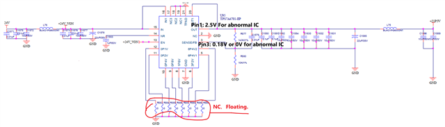
Strange phenomenon were detected by my me about the fb pin and output. Output will change to 2.5V and Vfb is 0.18V or close to 0v with the normal input voltage 24V. No abnormal heating points or burnt defect was detected on abnormal chips. Very strange, the Vfb voltage is abnormal. Once we replaced the abnormal TPS7A4701-EP with a new one, it works normally.

The input output specifications and the SCH are attached. Please kindly give me some insights about this?
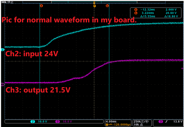
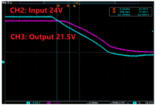
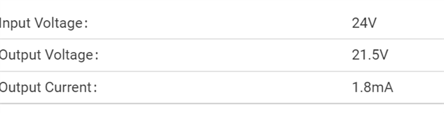
Input Voltage:

24V

Output Voltage:

21.5V

Output Current:

1.8mA

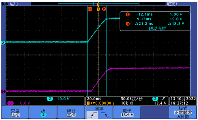
The vout voltage setup diagram for normal ICs (ch2).

Thanks ,

Marsh

  • Hi Marsh,

    I don't see anything that would cause this behavior if there wasn't some type of event that caused it. 

    Is this device power-cycled many times before the abnormal output observation? Is the abnormal output observed after the device has been operating normally or does it start behaving abnormally somewhat randomly?

    Is the 24V stable or does it move around or dip under 21.5V? 

    Regadrs,

    Nick

  • Hi Nick,

    1, What type of event would result in this kind of failure?

    I don't see anything that would cause this behavior if there wasn't some type of event that caused it. 

    2, 200 power-cycles(power on for 10s, power off for 30s) were conducted and no damage were detected.

    3, I'm not sure if input 24V is greater than output 21.5V always and forever. What will happen with input less than output? reverse current? Will this lead to failure definitely?

    4, Input has an initial voltage of 2V before power up, which means LDO will operate in UV condition for a short time. Will this be the root cause?

    Thanks

    Marsh

  • Hi Marsh,

    1. I would expect a reverse voltage to cause a failure like this. A reverse polarity from input to output can cause two consequences. The obvious one is that a reverse polarity can result in reverse current which can destroy the device. The other is that a reverse current that is insufficient to damage the device can get the internal circuitry into a state that causes the output settle to a different operating point. We would normally call this "latching" behavior. This can happen in many devices that do not have integrated reverse polarity protection because it is inherent to the architecture.

      There is a risk to reverse polarity in your schematic since there is a lot more output capacitance than input capacitance. 
    2. If this is a latching scenario, the device may not be damaged. The device can usually recover when power-cycled if it gets into a latching state. 
    3. It will not always lead to a failure if there is a reverse voltage. However, if a reverse voltage is expected it is normally recommended to use a low-Vf (less than 300mV) Schottky diode from the output to input to help provide a path for reverse current to flow that is not through the device. 
    4. It's possible that this minimum input voltage is resulting in the device not fully power-cycling, but I wouldn't say that it's the root cause. I would think that the root cause is a reverse voltage.

    Can you capture a power-down scope shot of the input and output? Something you could also try for testing purposes is to replace one of input caps with a resistor to help bleed off extra voltage when the board in powered down. 

    Regards,

    Nick

  • Hi Nick,

    Please review the power-down waveform. There is a such phenomenon reverse current flowing through the parasitic body diode. The voltage across the input and output is about 3V. Can we say that the reverse voltage is the root cause of the failure?

    Do you have any recommendation for the solutions? No PCB modification would be the best.

    Thanks 

    Marsh

  • Hi Marsh,

    I believe that this is the root cause. I would expect that if the input voltage can go all the way to 0V before powering back up, the device would have a fresh restart and would not exhibit this abnormal behavior. Fortunately the power down is slow enough that the device isn't damaged by this reverse current.

    With no PCB modification, I think your best option is to replace one of the capacitors at the input to help bleed off the remaining voltage after powering down. If the board is expected to be powered off on the order of seconds before powering back on, the resistor can be pretty large (and so the extra current is small). 

    Regards,

    Nick

  • Hi Nick,

    Thanks a lot for your input.

    I made a brief summary about this case. Can you please kindly help to correct if I made any mistake.

    1, TPS7A4701-EP is in "latching".

    Evidence1, we see the trigger for latching which is the reverse voltage observed on this part when powering down.

    Evidence2, the requirements for removing the latching is not satisfied, due to the remaining voltage on input before powering back up.

    2, Recommended workaround.

    Recommendation1, modify the PCB and add the anti-reverse protection.

    Recommendation2, replace one input cap with an resistor to bleed the remaining the voltage on input to help part have a fresh power-up.

    ------------------------------------------------------

    3, Questions for the condition of abnormal materials.

    A, You believe that the abnormal parts are in 'latching' and can recover, right? Because we didn't observed any hot point or obvious burning point on the part.

    B, Why you will make such an conclusion that power down is slow and device is not damaged. (Based on the facts 1reverse flowing time: 6ms; output capacitance 72.3uF; ΔVoltage 15V, we can estimate the reverse current to be about 180mA, can TPS7A4701-EP's body diode handle such a current?)

    Fortunately the power down is slow enough that the device isn't damaged by this reverse current.

    Thanks

    Marsh

  • Hi Marsh,

    Your summary looks good to me. 

    3. A. Yes, that is what seems to be happening. A latching condition will not cause extra power dissipation.

    B. This was an observation. Since you mentioned that the power was cycled 200 times without damage, I would attribute that to the relatively slow power down since there's a pretty good amount of output capacitance. We normally recommend limiting the reverse body diode current to 5% of the device's rated output current for reliable operation. For this device, that would be 50mA. Going beyond this 5% figure will not always cause failure, and in this case it does not appear to be causing damage. With that said, perhaps one more recommendation would be to reduce the amount of output capacitance to reduce the reverse current to help improve reliability. 

    Regards,

    Nick

  • Hi Nick,

    Thanks so much for your input. But actually till now, we still cannot identify if this is the root cause.

    For better identifying the root cause, we plan to design an experiment to repeat this issue stably. But still not clear about how to do. Can you kindly share your insights in repeating this error? 

    Regards,

    Marsh

  • Hi Marsh,

    To reproduce this, you need to create a reverse voltage condition such that reverse current flows but not so much that the device is destroyed. To do so, I would recommend powering the device and get it to a normal, stable operating point, and then bring the input voltage down under VOUT to create the reverse voltage condition. Then after some time (a few to 10's of ms I would think), bring the input back up. The knobs you have to tweak are:

    1. VIN ramp-down rate
      1. If you are using an arbitrary waveform generator + buffer, you can adjust the ramp rate such that the input falls faster than the output discharges back to the input, but not so fast that too large a differential voltage exists
    2. Input/output capacitors and their ratio (i.e. how much larger COUT is than CIN when your bring the input down)
      1. start with a smaller output cap to avoid large reverse current and increase in size if it falls too quickly

    Regards,

    Nick

  • Hi Nick,

    I have received the EVM and abnormal part and I find something weird with the experiment.

    1, The CRU( customer return unit) can output 20.4V with 24V input and no load. see pic1. But it's output ramped very slow and weird. Pic2 is the EVM unit performance, ramp up beautifully.

    2, When I add an 200Ω to CRU, the output voltage will go down rapidly, and the detail waveform(pic3) shows it's a biased sawtooth.

    Questions:

    1, Does this mean that the pass-FET is broken?

    2, Is this the consequence of reverse current?

    Something wrong, that pics cannot be attached here. I have sent you an email.

    Thanks 

    Marsh

  • Adding the images for easier tracking.

  • Hi Marsh,

    This looks like a damaged pass-FET. It is difficult to say how it got damaged, but yes a reverse current could cause this. 

    Is the sawtooth waveform showing the device output when there is a load applied? Does the device still recover to regulation from a sawtooth output when you remove the load?

    Regards,

    Nick

  • Hi Nick,

    Yes, the sawtooth with average voltage 1.5V showed when applying the load, and the output voltage went back to 20.4V when I removed the load.

    Thanks,

    Marsh

  • Hi Marsh,

    I'll get back to you tomorrow about this. 

    Regards,

    Nick

  • Hi Nick,

    Any update?

    Marsh

  • Hi Marsh,

    Sorry for the delay. 

    Were you able to reproduce any of the behavior by doing the experiment I outlined above? I think it is evident that the abnormal device has a damaged pass-FET, so at this point all you can really do is try damaging a good one in the way that we have theorized and see if it shows the same behavior. 

    Regards,

    Nick

  • Nick,

    Just as I mentioned above, the sawtooth appeared only when I applied the load, and the output voltage went back to 20.4V when I removed the load.

    The fact is CTM repeated 200+ experiments and no issues detected. I'm thinking if the damage were accumulated with repeating time ramps up. What I mean is that the reverse current is bring damages but it will not just destroy the part immediately. It's hard for me to convince CTM if there's no repeating issues detected.

    Marsh

  • Hi Marsh,

    What I mean is that this device is already damaged, so there isn't anything we can do to prove what caused the damage, unless an FA-type of analysis is done on it to see exactly where the damage is inside the die. 

    So this is an isolated incident where they have not replicated it? I was under the impression that this was happening with many devices. 

    Regards,

    Nick

  • Nick,

    I agree with your point. The fact is many devices damaged at the field, and no device damage replicated in LAB.

    They really want to replicate in LAB and then close this thread.

    I have recommended them to add diodes and/or other circuits to prevent the reverse current.

    Marsh

  • Hi Marsh,

    Nick will get back to you asap, thank you for your patience

  • Hi Marsh,

    I don't really have the bandwidth to run bench tests right now. Since you already have a bench set up, can you try the test that I outlined above with a fresh, undamaged device? 

    Regards,

    Nick

  • Hi Nick,

    Hope you have enjoyed your day!

    One quick question. Do you have any LDO recommendations with reverse current protection for the below requirements?

    Best Regards,

    Marsh

  • Hi Marsh,

    TPS798-Q1 fits this requirement. I think this is the only option here.

    Regards,

    Nick

  • Hi Nick,

    Thanks! Helpful!

    Marsh