A related question is a question created from another question. When the related question is created, it will be automatically linked to the original question.
If you have a related question, please click the "Ask a related question" button in the top right corner. The newly created question will be automatically linked to this question.
LP8866-Q1: LP8866 design tool and Schematic review
FSW = 400KHz; the frequency multiplication after spreading is affected at 800KHz, 1200KHz, 1600KHz! At present, it is confirmed that it is affected by LP8866. Customers have tried FSW = 200KHz, 303KHz, and 500KHz frequency multiplication, all of which affect this frequency band.
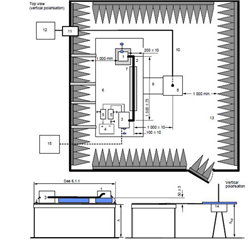
Test method CISPR 25 / Radiated emissions from components/modules - ALSE method
In addition, I would like to ask what is the upper limit of RG in Datasheet Table 8-3?