This thread has been locked.

If you have a related question, please click the "Ask a related question" button in the top right corner. The newly created question will be automatically linked to this question.

UCC27282-Q1: Requirements about Vdd

Part Number: UCC27282-Q1
Other Parts Discussed in Thread: UCC27282, LM317MQ

Hi Team,

There is a question here about UCC27282-Q1. Is there any requirements for voltage on Pin1 Vdd? We promote UCC27282-Q1 to alt Diodes DGD05473FNQ. But UCC27282 needs Vdd greater than 6V. So we promoted LM317MQ to step down the voltage from 12V battery to supply UCC27282. After verification from customer side, Vout of LM317MQ is like below yellow curves when load current varies from 50mA to 500mA. Peak to peak voltage is about 300mV and there is ramp up and down in the outputs. The average value of the curve is about 7V.
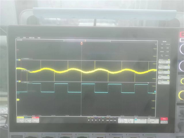
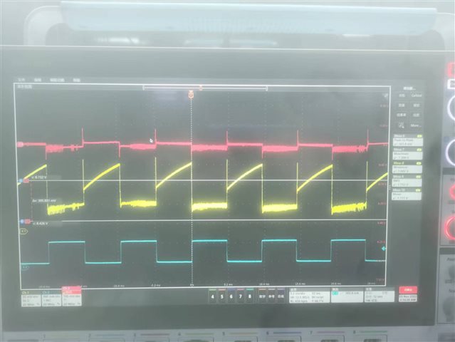
Would you pls help to confirm whether our UCC27282 can work normally in this condition?

Thanks a lot.

Wenmin Hua

  • Hello Wenmin,

    Regarding the question about the ripple on VDD, I did confirm during the UCC27282 validation testing that the driver VDD was tested with high levels of VDD noise beyond what you show in the results. The UCC27282 is tolerant of VDD noise within what you show and there was no effect on the driver operation.

    I do have one question however. It seems there was a concern that the UCC27282 needs a minimum voltage of 6V but there was a linear drop down regulator added. Is there a concern about VDD being too high in some cases?

    Regards,

  • Hi Richard,

    Thanks for confirm. As for your question, it is exactly the reason we add the LDO. Because the 12V battery in automotive will up to 38V when load dump. This value is over the abs maximum of Vdd. Would you pls give some suggestions about this application ?

    Thanks a lot.

    Wenmin Hua

  • Hello Wenmin,

    For the case where VDD can exceed the recommended maximum rating, adding a regulation circuit on VDD to limit the maximum voltage would be required. The solution you have should serve the purpose of limiting maximum VDD. There may be simpler, lower cost methods such as a zener and transistor regulator, but you would have to verify if this would work with the input voltage range to the regulator.

    One thing to note: The VDD regulator does not need to support the peak current of the UCC27282 driver outputs. The driver outputs will have high peak currents but they are short duration and are souced from the VDD and HB capacitors. The regulator only has to support the average current into the driver which can be estimated by: Iavg= Fsw x Qg where Qg is the total gate charge of the power switches on HO and LO driver outputs.

    Regards,