A related question is a question created from another question. When the related question is created, it will be automatically linked to the original question.
If you have a related question, please click the "Ask a related question" button in the top right corner. The newly created question will be automatically linked to this question.
I want to confirm if 3.3Vout has same phenomenon? the sensitive analog traces such as VOx, VFBx, should be placed away from high-voltage switching nodes such as LLx, DRVLx, DRVHx and VCLK nodes to avoid coupling.
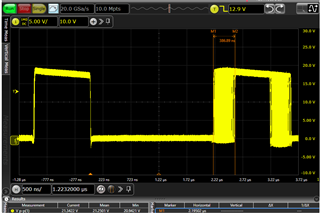
Thank you for the precautions you provided. In addition, under the same test conditions, the low-level jitter of the 3V Phase side is smaller. We want to understand some theoretical questions, please help to answer the following questions, thank you.
Test conditions: DC 18V, output 5V/8A, 3V/8A
1. What is the cause of Phase low-level jitter? Is it the inherent jitter inside the IC or is it caused by external factors?
2. What external factors may cause such jitter (device selection or PCB layout)
3. Are there any specific requirements for the threshold of Phase low-level jitter? For details, please refer to which indicators in the specification
4. If this jitter is too large, what is the specific phenomenon that may be caused?