Other Parts Discussed in Thread: PMP6712
Hello,
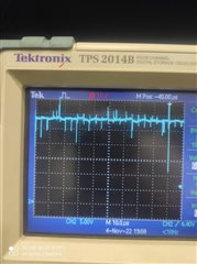
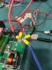
I have a very similar design to the PMP6712 that I made using "ucc28950", in this design, when I try to load the output, the output voltage deteriorates a lot, and my Q4 mosfet, pictured, gets very hot
This thread has been locked.
If you have a related question, please click the "Ask a related question" button in the top right corner. The newly created question will be automatically linked to this question.
Hello,
I have a very similar design to the PMP6712 that I made using "ucc28950", in this design, when I try to load the output, the output voltage deteriorates a lot, and my Q4 mosfet, pictured, gets very hot


Hello,
I would suggest double check your Input H Bridge and Output H Bridge drivers are driven by the correct outputs. If they are not it could cause circuit misbehavior.
You may want to study the COMP, CS and the voltage across the primary of the transformer as well. To make sure your control signals are as expected.
Regards,
Hello,
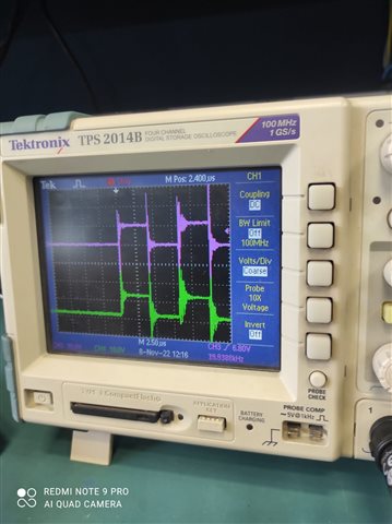
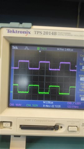
while there is no 270V supply in the system, it is only supplied with 12v, the q4 and q5 gate signals do not conflict, everything seems normal.
When 270V is turned on, the output is underloaded, the system is running in "burst" mode, but the q4 and q5 gate signals overlap, is this normal ? I think it shouldn't be like this ? what do you think is the reason ?
Best regards,
Hello,
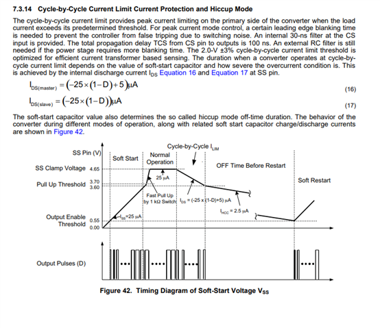
If your design is bursting and the output is dropping out of regulation you could be hitting over current protection.
If you study the CS pin and SS you should be able to determine if this is the case.
The following section from the data sheet describes cycle by cycle current limit and over current hiccup mode protection.
This should help you evaluate if you are going into hiccup mode protection.
Regards,
Hello,
when I look at the outputs of the tina program below, I observe that my signal is correct, when I examine the output with an oscilloscope while loading, can we connect it to the "hiccup" mode so that the output voltage reacts as if it has dropped, even though the output voltage has not dropped?
Hello,
It is good to know that your H Bridge drive is correct.
Have you look into the following suggestions?
If your design is bursting and the output is dropping out of regulation you could be hitting over current protection.
If you study the CS pin and SS you should be able to determine if this is the case.
The following section from the data sheet describes cycle by cycle current limit and over current hiccup mode protection.
This should help you evaluate if you are going into hiccup mode protection.

Regards,
Hello,
I also have attached a link to an application note that reviews how to design a phase shifted full bridge with the UCC28950. There is a link inside to an excel design tool that goes with the application note. You can use the application note and excel design tool to double check your design.
https://www.ti.com/lit/pdf/slua560
Another tool that you might find helpful is the UCC28950 600 W evaluation module. The following link will bring you to the user's guide and you can buy the EVM from ti.com. https://www.ti.com/lit/pdf/sluub02
You can study the EVM and compare COMP, CS and gate drive waveforms and compare it to your design. This could be helpful in determining why your design is not achieving full power as well.
Regards,
Hello,
Hello,
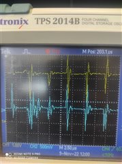
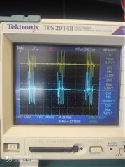
There is lots of noise on your SS and CS pins. If this noise is real it will cause your circuit to misbehave.
Did you take your measurements referencing the UCC28950 IC ground? If so you may want to retake the measurements.
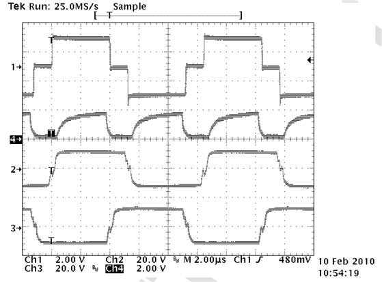
You current sense signal does not look correct. Do you have your CS transformer setup correctly?
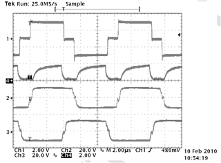
The following waveform shows what your CS signal should look like. CH1 is the voltage across the primary of the transformer.
CH2 is the gate of FET QA, CH3 is the gate voltage of FET QB. CH4 is the CS sense signal. Please note these waveforms were taken from a design that used gate drive transformers. However, the CS signal is correct.
You also could possibly have a layout issue. The user's guide of the EVM previously reference has the layout in it that was used in the EVM. You can use this to compare to your layout to see if there are any major differences. The data sheet also gives guidance on how you should layout the board.
I also have attached a very good application note written on layout. It is actually written for op-amps but it is one of the best papers that I have read on layout and found the information very helpful when laying out power supply PCBs. I thing you will find this information useful.
Op Amps for Everyone Chapter 17.pdf
Regards,
hello,
The problem of output voltage dropping as it loads is gone, but the q4 still gets very hot in any case, could it be because of "L1,L2,L3"? its equivalent inductance is 270nH, although it seems that way in the calculation, I think it is too small
Hello,
The clamping diodes are used to redirect current when the design comes out of freewheeling. The shim inductor current (L1, L2,L3) will be different than the primary transformer current when it comes out of freewheeling. These diodes give a place for the difference in current to go. So put D3 and D6 back in the circuit.
Having FET Q4 get hot without the other ones is kind of strange. I wonder if that FET got damaged. Could you try replacing it with a new FET to see if it fixes the problem.
Regards,
Hello,
The shim inductors should not cause one FET to get hot. You should study the transformer current to see what it looks like; as well as, the current through the H Bridge FETs to try to figure out why Q4 is getting hot.
Regards,
Hello,
when I connected the "shim inductor" value of 3.3uH instead of 270nH, the overheating problem of Q4 disappeared on its own, but my shim inductor gets very hot after a certain current, I wonder if there is a type of inductor that you recommend for this, I use the product linked below.
Hello,
If your shim inductor is getting hot it might be saturating. Find and inductor that is rated for the RMS current that you putting through it. This will prevent saturation.
The following link will bring you to an application note on how design the UCC28950 in a phase shifted full bridge. There is a section on how to select the shim inductor.
https://www.ti.com/lit/pdf/slua560
Regards,
Hello,
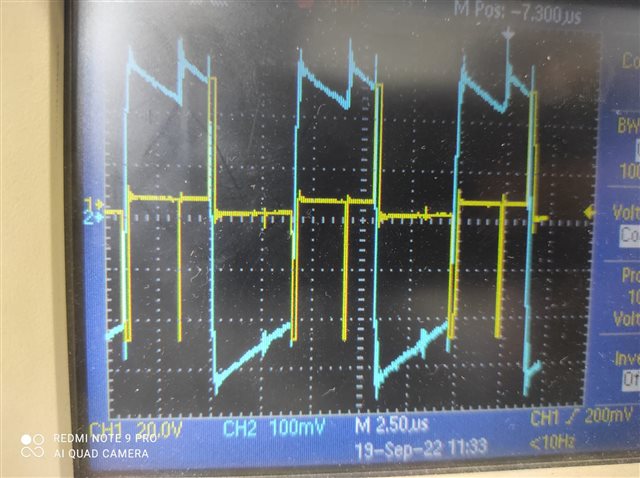
The following figure shows the current flowing through the coil with a blue signal The equation should be established as 50mV=1A, When 20A is drawn at the output, a current of about 2A should flow from the 270V input, It also looks like this at the power supply, although what can explain the appearance of such a current value?
Perhaps the answer to all the heating questions is due to this current, could the reason for this current be that the primary inductance of the transformer is low ?
Regards,
Hello,
The current in your coil/transformer should be similar to the primary current in the transformer. This current does not look correct for a phase shifted full bridge. You are correct that it could be contributing to the heating.
To you have a full schematic that you could share that I can review?
Regards,
Hello,
I reviewed your schematic and can see any major errors. However it looks like you are trying to use adaptive delay. Your E and F FET driver timing looks like it might be off. I would recommend trying to use a fix delay approach as recommended in SLUA560.
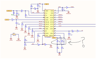
Your current waveform does not look correct. There has to be something different than what you are showing in the schematic. When A, C and F are on at the same time. The CS signal should be the reflected output current plus the change in current in primary magnetizing inductance (Lm), shim inductance (Ls) and output inductance Lout.
Your waveform only shows a current down slope Also it looks like that when the blue waveform is positive it is being shorted out as well.
This waveform looks like the H Bridge is loading the output. There is a never a positive inductor current slope.

There is something wrong in your schematic compare to the waveforms you are presenting. I would double check your schematic vs your design.
Your schematic also does not seam complete. The reference designators are incomplete and reference by ? marks and not number sequentially.
I suggest the following:
1. I would suggest completing your schematic with sequential reference designators it will make it easier to trouble shoot the design.
2. Compare your schematic to your actual design
Regards,
Hello,
Hello,
1. The app note sets the ADEL and ADELEF pin off the reference voltage. With this method you can use the application note to setup the timing.
2. The other option is tie ADEL and ADELEF directly to ground. Then you need to follow the equations in the data sheet for setting the FET turron delays.
3. Approach 1 and 2 will work for a fixed delay approach.
4. Adaptive is only used by 1% of designers in an attempt to remove body diode conduction from the H-Bridge. However phase shifted full bridges generally have a high voltage front end and removing H Bridge body diode conduction does not provide much benefit.
Regards,
Hello,
I did not see other errors in you schematic. However, you current waveforms indicate that the schematic may not match the actual design. I would double check your design vs the schematic as well.
Regards,
Hello,
It might be causing the short seen on the primary in your current waveform.
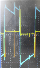
The more I look at this waveform it looks the converters duty cycle might be off. It only shows mostly output inductor discharge current. It looks like as soon as the design comes out of freewheeling and the transformers input voltage polarity is changed the duty cycle terminates. You had mentioned that the design regulates the output voltage. With this current waveform I would think it would not.
In your design what should the duty cycle be based on the transformer turns ratio?
Was the current waveform that you had taken under any load?
Regards,