This thread has been locked.

If you have a related question, please click the "Ask a related question" button in the top right corner. The newly created question will be automatically linked to this question.

LM25149: power-up fail / high consumption on AEFVDDA

Part Number: LM25149

Hi team,

we recently got issues with LM25149 behavior during startup. 
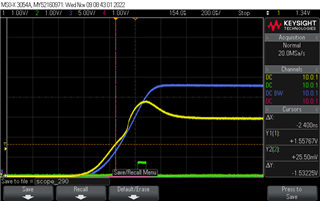
Vin:24V

Vout 12V

Fsw 600kHz

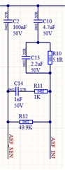
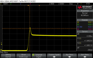
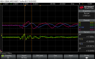
Symptom is that board fails to power-up. Power consumtion is either 22mA or 160mA (rest of the board is pretty much powered down). Trying to isolate problem we found that issue is caused by AEF probably overloading the Vcc.If R461 is desoldered, board starts normally. The pin does not seem to have a short to GND pad when measured with ohm meter.

The C565 was verified on the first failing board and nothing suspicious was found. Seem to be really in the IC itself. Today, a second board developed same issue. In both cases, this happened when board was powered on after being powered off for some time, not when runnning. Before failing, nothing was done around this part of circuit, so unlikely a scope probe slip.

Any idea what could cause this behaviour? Would it be possible to send the failing chips for analysis? 

We currently run two batches of boards up to now. It was not observed int he first batch that was deeply verified, but there was a limited number of samples (less than 5).

In this second run, two boards developed this issue. This was likely assembled from a different reel. Both batches of chips were obtained from TI. Difference between two batches that come to mind are COMP loop componnet values and aef values, otherwise not much was changed. 

I will tomorrow investigate heatthy board for any clues, but in the meantime any advice is appreciated.

Thank you


  • Hi Petr,

    Can you isolate whether it is an IC problem or board level problem?

    That is can you swap the IC on a working board and failed board, and see if the problem persists?

    It does seem like AEF is current limiting VCC, 22mA is normal but 160mA is abnormal, thats almost like the INJ pin is GNDed or very low impedance to SEN. 

    Let me know if it's an IC level problem, that is if a failing IC fails on otherwise working boards.

    -Orlando

  • Hi Orlando,

    The first board went for rework with a fresh IC and is not back yet, the second board I keep in "dead" state for now. 

    I tried to verify impedances beween INJ/SEN nodes to GND and to neighbouring pins but I don't see any suspicious values. I also tried removin D19 but that did not help.

    I found that the difference between 22mA and 160mA is the power ramp up. If input is ramped from 0 to 24 by enabling lap supply consumption is 22mA, if by hard plugging the power input connector that falls into 160mA consumption and IC heats up.

    When IC is disabled by tying EN node to GND before turning on the input power supply, the board consumption is about 1mA.

     I will try to investigatre the board a little bit more, if you have any additional comments while we wait for rework they are appreciated.

    Thank you


    Here is a snapshot of Vcc node during startup:

  • Hi Petr,

    That VCC is strange, it doesn't even make it to 5V before falling off.

    Is the output regulated? Can you take the same scope shot of VCC, VOUT, PG, and CNFG?

    With your CNFG setup the AEF should not enable until after the output is regulated and PG is up.

    But it would appear as if AEF is enabling and sinking current before VCC is fully up. 

    It could be the PG pulldown is delayed during the hotplug, lets see what you get on the scope shot.

    The 1mA when disabled is a bit suspect, the upper enable resistor R453 should only dissipate 240uA.

    Double-check the input current with a multimeter or something else, as some power supplies are not accurate at mA scale.

    Let me know,

    -Orlando

  • Hi Orlando,

    thanks for the suggestions, i will take the snapshots tomorrow. But today I tried with D19 removed but behaviour was the same, however that was on already "faulty" board. 

    Today I managed to reproduce the issue on one other board so I could try to rework the chip. I can now confirm that if chip is swapped for a fresh one, issue disappears. Then i was able to reproduce once more with a hot-plug, again same symptoms. After that, another IC was soldered and I was not able to reproduce again. Now the board looks pretty immune so I was actually able to take some snapshots.

    I aimed on AEFVDDA and VCC. During hotplug, there seems to be some transient actually exceeding the pin rating on some occasions. I will tomorrow doublecheck that this is scope related issue but attaching the snapsot anyway if it would ring some bells.

    Magenta-supply connector

    Blue - chip Vin (after 3.3uH inductor)

    Green - Vcc

    Yellow - AEFVDDA

    This is during unplug event, afterwards Vin starts to fall. I looked there as well, but nothing suspisious there after these events. 


  • Hi Petr,

    That waveform is different from the previous VCC wavefome.

    Will you be able to get a scopeshot of the startup or issue?

    Let me check with the designer, I see we have AEFVDDA pin max as 5.5V, however the VCC absmax is 6.5V so I would expect AEFVDDA to be tolerant to 6V.

    -Orlando

  • Hi Orlando,

    The picture in first post is from "dead" board during power-up. 

    The picture I shared in the latest post is from power unplug on a board that was re-worked with a fresh IC. On this board with a new IC, I am not able to reproduce this issue anymore. Looks like if some ICs were more tolerant than others? 

    Here is a picture from a dead board during power-up requested earlier. To your question - the output is not regulated. 

    Yellow - Vcc

    Green - CNFG

    Magenta - PGOOD

    Blue - Vin

    (mind the different voltage scale, the Vcc does not actuaslly power up before Vin)

  • Hi Petr,

    That dead board looks like the VCC is not coming up to 5V.  I'm assuming removing the AEFVDDA resistor will allow this VCC to reach to 5V?

    The configuration time seems a bit long but it does seem like it is working.

    The PG is not coming up so the AEF should not be enabled, I'm not sure why the AEF would be consuming current.

    Are you able to read the top markings on the ICs? 

    Let me know,

    -Orlando

  • Hi Orlando,

    correct, if AEFVDDA resistor is removed, board comes up normally in both cases.

    The topside markings of two affected chips are: ( " | " denotes new row)

    1. LM25149 | TI 108 | A9FN G4 

    2. LM25149 | TI 258 | AXJ5 G4 

    Any idea about that Vcc overshooting nominal value during unplug in the scope shot I posted before?

    Engineering sample run date is approaching and we would like to have some understanding of possible sources. It is ok to take the discussion into PMs or email if some IP is involved.

    Many thanks

  • Hi Petr,

    Based on the top marking the silicon revisions are the same.

    I tested a hotplug on the EVM, the VIN does not ring like that. 

    I cannot see your AEF inductor, however from your schematic it does not appear as if your filter is damped on the power stage side.

    For any LC there should be damping to prevent ringing or resonances.

    We used CD and RD for this damping. See section 9.1.1.5 in the datasheet.

    See appnote as well: https://www.ti.com/lit/an/snva538/snva538.pdf 

    I did talk with Systems, the AEFVDDA absmax is 5.5V and not tolerant to higher VCC.

    I suspect that VCC ringing did damage the AEF circuit (which is separate from the controller).

    We are not sure why some ICs are more tolerant than others, but that VCC is not acceptable for AEF.

    I will add a note to the AEFVDDA about potential clamping needed.

    However if your VIN is properly damped then VIN and VCC should not ring as such.

    Hope this helps,

    -Orlando 

  • Hi Orlando,

    I did some measurements with scope and I think i made a reliable reproducer.

    The whole situation seems to a product of transients on input connector that subsequently gets into INJ/SEN pins. In the schematics above, LM25149 get's enabled at around 14V, meaning that before input supply reaches that, internal regualtors are disabled. And that seems to be the point where most of the damages happens if there are transients on power lines. 

    I modified the enable threshold to 4V so Vcc (and consecutively AEFVDDA) gets enabled very early and my reproducer stopped blowing the chips. Before, I was able to blow up the chip on first or second try, now it seems to be very resilient (I will try to test on more boards). 

    We do have a inrush current limiter circuit there on the input of device. It has some practical limits and I realized that when it is inactive, it is when most of the damage happens, which lead me to findings above. 

    I would love to hear some insights to behaviour described above and if we can do more to protect the device. It is fine to reach through PM if some IP is involved, however I would like to get deeper understanding of the issue.

    //EDIT:

    I tried to modify dev kit and I am a bit more sure that what I state above is correct. I am able to reproduce the issue by partly modifying the EVB. just change injection branch:

    C3=4.7uF

    2.2uF in paralllel with R1

    R454=7.68k

    Vsupply=24V (5A current limit)

    This creates low impedance path to INJ pin. Without 2.2uF I was not able to reproduce issue, but while fiddling positive banana plug on lab supply (and having the 2.2u there) the death was more or less instantial. 

    Thank you

  • Hello Petr,

    Large capacitive coupling to the device's pins, along with a very fast DV/DT events (such as Hot plug) will cause large transient voltages to appear on the device pins. 

    With the above conditions without some front-end control, like a hot swap device, you will need to minimize the electrical coupling to the device pins and/or install a clamping device close to the device pins to protect against electrical over stress.

    Hope this helps.

    David,

  • Hi David,

    Many thanks for response. Regarding transients that's what I understood during my testing as well, but I was wondering if the Vcc/AEFVDDA not being up could make the device less resilient to such events? 

    Secondly, is the INJ pin rail to rail with regards to AEFVDDA? We need it to understand demands on the clamp device, as finding some that withstands 5.3V (Vcc max from datasheet) and clamps at 5.5V (INJ nore max input voltage) might be quite hard.

    Regards

    Petr

  • Hello Petr,

    I agree if pins are not loaded, this will likely make the magnitude the voltage greater.

    The AEF amplifier is a rail to rail amplifier WRT to AEF_VDDA

    Hope this helps,

    David.