

Dear Experts,
Question-#1:
I would like to know layout priorities for FB components (R1, R2) and passives of the internal error amplifier (R5, C5, C6).
I know that it is desirable to place them on the same layer. However, in our situation, one of them must be placed on the opposite side. Which one should be placed on the bottom layer to have less effect on the characteristics?
Question-#2:
About FB trace length impact. Typical application (Fig-3) showed that R1, R2 = 681k, 107k. We might choose 1% tolerance resistors for them. And they will be tied with 0.2mm width & 1oz Cu trace (Trace DC resistance is about 0.002 ohm / mm) between dividing point of R1 & R2 and FB pin (I don't think it will be not exceeded 10mm). How many millimeters of FB trace length do you think is acceptable in this situation? There are no noise sources in the surroundings.
Fig-1
Fig-2
Fig-3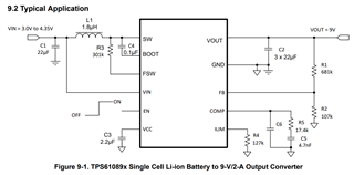
Regards,

-
Ask a related question
What is a related question?A related question is a question created from another question. When the related question is created, it will be automatically linked to the original question.
