I am using The controller for a 5.2 V and 3.3 V converter.
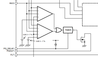
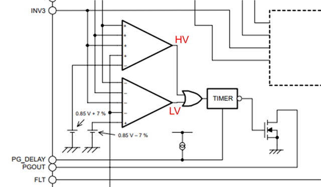
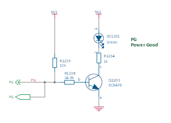
I have tied the 3.3 V to INV3 (pin 15) to enable the PGout (pin 16) once termination voltage has been reached.
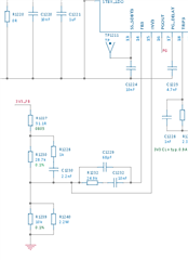
The schematic above shows the divider for 3V3 to get 0.85 V at INV3. PG only ramps up to 2.5 V due to the pull up on the open drain of PGout being a divider to a bjt to enable a Power on LED. (A FET will replace the BJT)
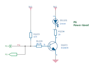
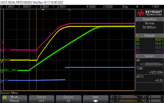
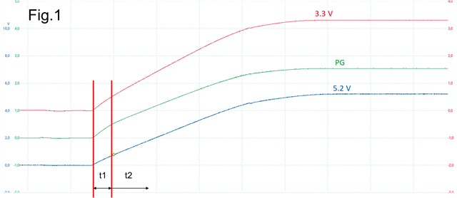
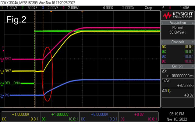
However, the PGout pin begins ramp up in sync with the 3.3 V supply. (This is with PGdelay open: 4.7 nF cap shown in schematic snippet removed) see the figure below for osc. capture.

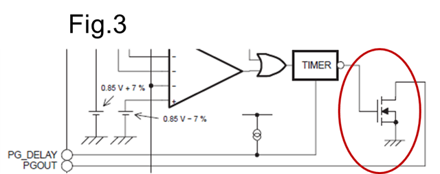
Only two converters are used 1 and 3, therefore i have tied SS_STBY2 and STBY_LDO to GND. therefore these should not effect the comparator as shown on page 8 of the datasheet used to enable the PGout signal.
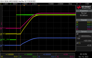
the delay function (PGdelay) works well if i want to ensure that 3V3 is stable before enabling the supplies downstream as shown in the figure below with an 8.2 nF cap connected to PGdelay.

I am thinking that there is something wrong with the design as this component has been around for approximately 20 years and this issue has not been raised, but up to now, my PG ramps up with the 3.3V.
Is this something that has been seen before.
Kind regards,
Russell