This thread has been locked.

If you have a related question, please click the "Ask a related question" button in the top right corner. The newly created question will be automatically linked to this question.

BQ25890: EMI issues, ~1.5 MHz. Design review

Part Number: BQ25890

Hi, 

We just performed a pre-test of our product, and we have a problem passing the radiated emission test. Could you please perform a design review? I would appreciate to have it private if that's possible. I can give you some information to begin with. 

Our product consists of two parts, both have the BQ25890 inside. We performed both radiated and conducte testing of both parts. See figures below. 

Part 1 charges its own battery and provides charging power to part 2 when part 2 is docked to part 1

Part 1 battery is only charged when USB is plugged in.

Part 2 is the main unit and its battery is either charged by part 1, when prevoiusly mentioned docking, or when USB is plugged into part 2.

Part 1 radiated emission:

Situation 1: Part 1 has USB plugged in, and Part 2 is docked to it, hence part 1 is charging its own battery and providing charging power to part 2. 
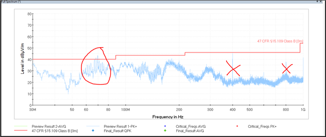
Please ignore the 400, 600 and 800 MHz spike, those are known unrelated issues.

We have a collection of spikes aorund 60-80 MHz and the spacing between them was ~1.5 MHz.

Situation 2: Part 1 providing charging power to part 2, USB not plugged in. Hence, the battery in part 1 is charging part 2:
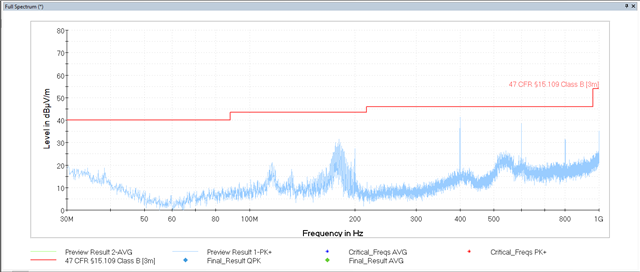
Nice and clean!

Situation 3: Part 1 has USB plugged in, and part 2 is NOT docked (not present in chamber). Hence, only charging its own battery.
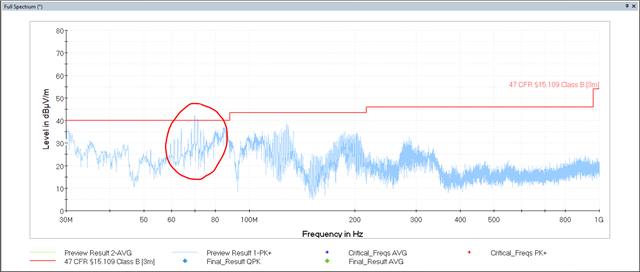
Still ~1.5 MHz spikes. 

Part 1 conducted emission:

Situation: Part 1 is charged through USB. Part 2 not present. 
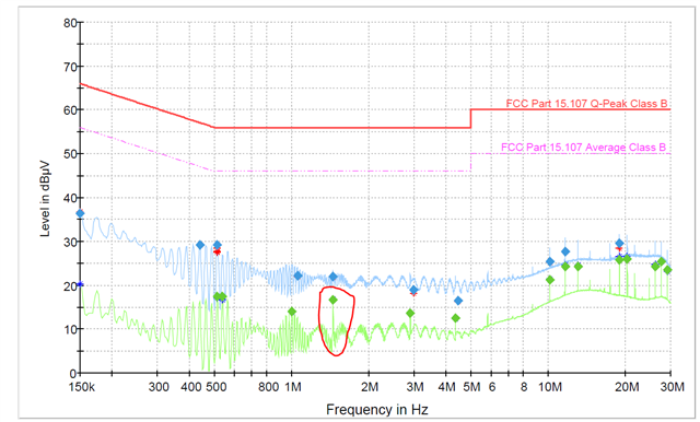
We can see the presence of ~1.5 MHz. And, alot of other spikes in the upper frequencies.

Part 2 radiated emission:

Situation: Part 2 is charged with USB plugged in. Remember that part 2 also uses BQ25890. Part 1 is not present in chamber.
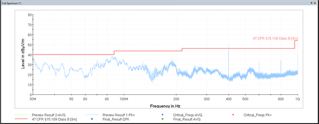
Here we don't see any ~1.5 MHz spikes. Although the 80-90 MHz is quite high. 

Part 2 conudcted emission: 

Situation: Part 2 is charged through USB. Part 1 not present. 
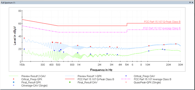
Ther are no spikes at ~1.5 MHz, and the upper frequencies are also quiter. 

The schematic for these two BQ25890s are the same in terms of inductors and capacitors, there are some differences with certain discrete signals and the voltage input. However, the PCB layout is different. So I think theres something fishy about the layout on Part 1. 

Can you please help me out here?

Best regards, 

Sindre Georgsen

  • Hi Sindre,

    As a first step please double check the schematic / layout guidelines located here and also in the datasheet Section 12

    If you would like to share your layout in private I can open a separate message contact with you. Please accept my request if you would like to proceed with the private share.

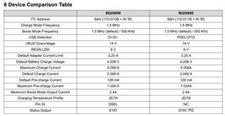
    My immediate suspicion is that there may be an issue with your switch node or something related to that part of your design. The BQ25890 has a switching frequency of 1.5 MHz (typical) which would fall in line with the spikes you are observing.

    Regards,

    James

  • Hi Sindre,

    I would recommend that you try adding a 1nF capacitor close to VBUS pin and a 1nF capacitor close to the PMID pin.

    Also, try adding an RC snubber before L1 on the SW node (as close to SW as possible). You can check the switching waveform using a high bandwidth oscilloscope and look for any noticeable ringing behavior that might inform your component choice.

    With these additions, the goal is to reduce the potential EMI source at SW node and for the input loop.

    Regards,

    James

  • Hi James,

    Thank you for your input. Your suggestions are also noted in the document "bq2589x/ bq2419x / 29x Layout Recommendations" found here: /cfs-file/__key/communityserver-discussions-components-files/196/bq2589xbq2419x_5F00_29xlayoutandEMIrecommendation.pdf so I take it that there was no immediate issues with the layout?

    I will implement your suggestions in the beginning of next week and revert back with result. 

    Regards, 

    Sindre

  • Hi Sindre,

    Correct, I did not see any immediate issues with the layout at this time.

    Regards,

    James

  • Hi James, 

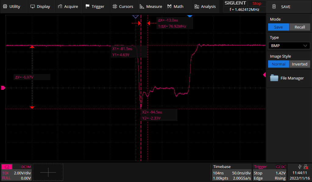
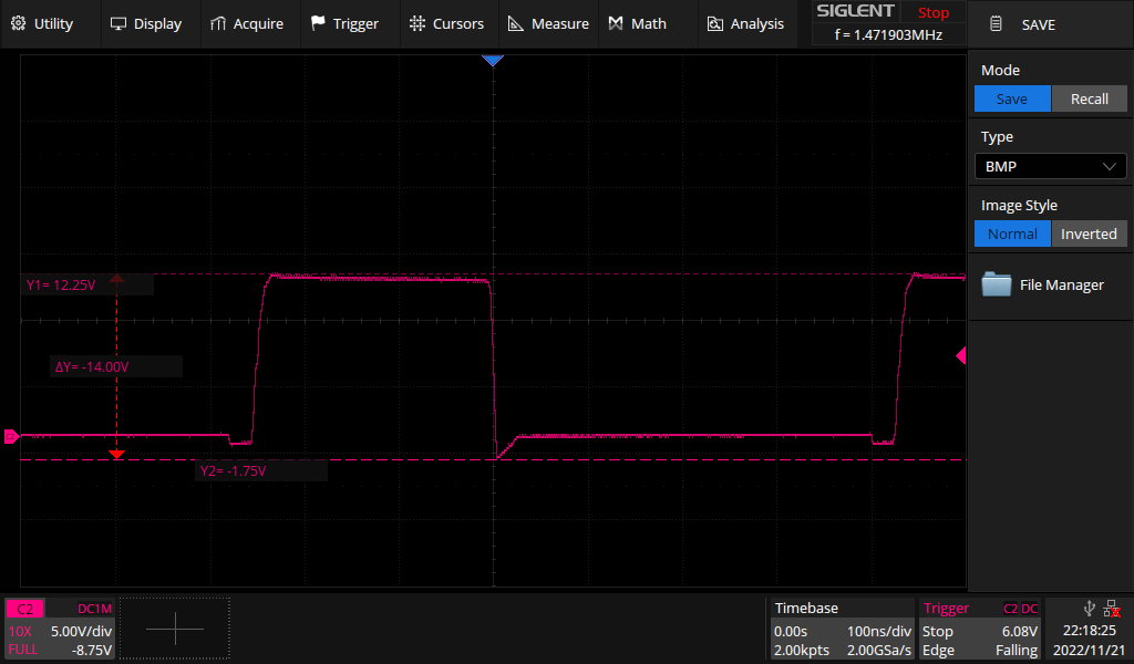
    I have now added 1nF to PMID and VSYS. And with two different USB-C wall adapters (one ouputting 5V, and the other putputting 12V) the SW node look like this:

    5V USB input:

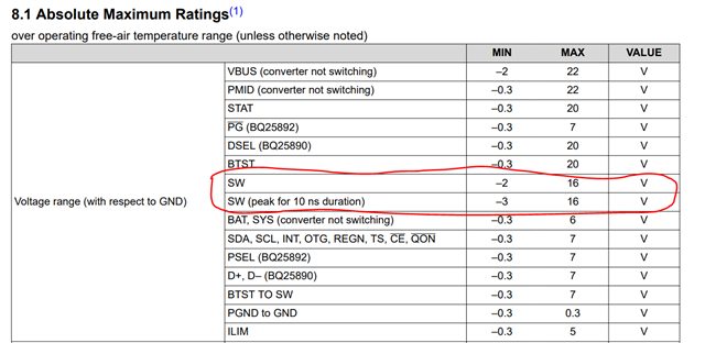
    There isn't much ringing on the high end, but on the low end the voltage goes as low as -2.3V which is at the below the low end of absolute maximum rating for SW node: 

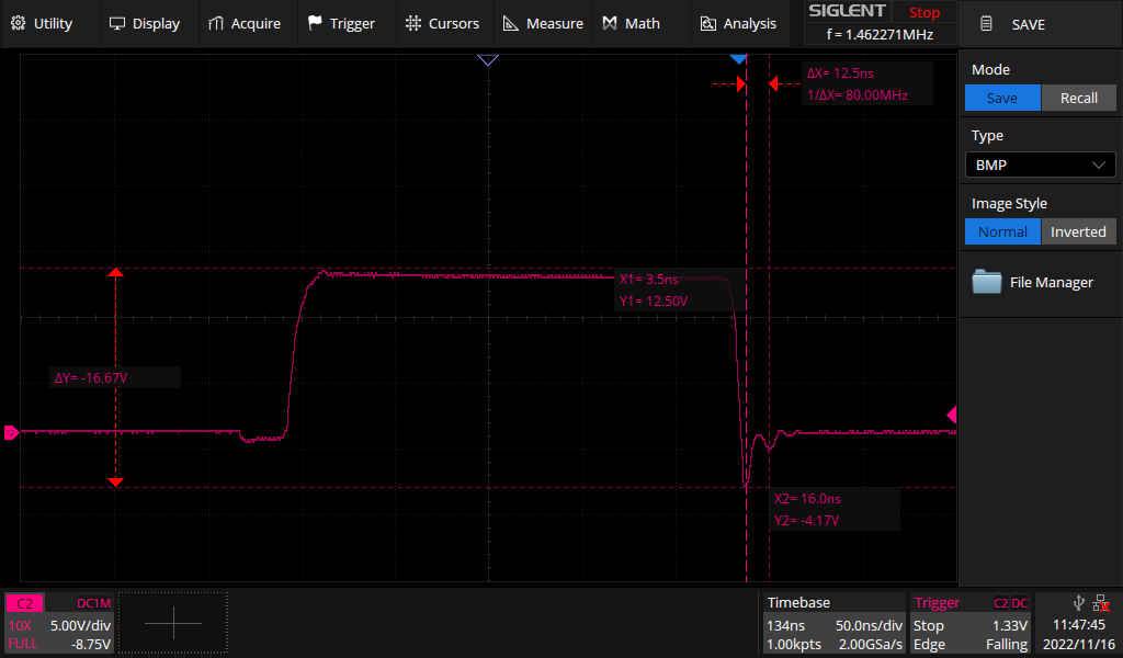
    12V USB input:

    With 12V USB input the SW node goes as low as -4.17V which definetly is below the absolute maximum rating. 

    I haven't measured without the added capacitors yet, I will do that tomorrow. 

    My scope is rated for 350 MHz only, and so are the probes. There might be some inaccuracy in the measurement related to that. 

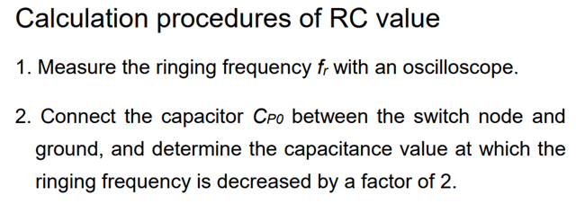
    I tried to find the snubber values by following this guide: fscdn.rohm.com/.../buck_snubber_app-e.pdf

    As a starting point I tried a 500pF (two 1nF in series) capacitor between SW node (before the inductor) and GND to find a capacitor value that halfed the ringing frequency but that really destroyed the chip. It got really hot and after a few seconds it shut down. It didn't start up again after cooling it down. So next step is just to add a 1nF and 2.2R resistor as a snubber without finding the optimal values. Just to see if that helps (on another working unit). 

  • Hi Sindre,

    Let us know what you find when you add the RC snubber and also how the SW node responds without the added capacitors as you mentioned.

    Regards,

    James

  • Hi James, 

    I have made some tests with a snubber:

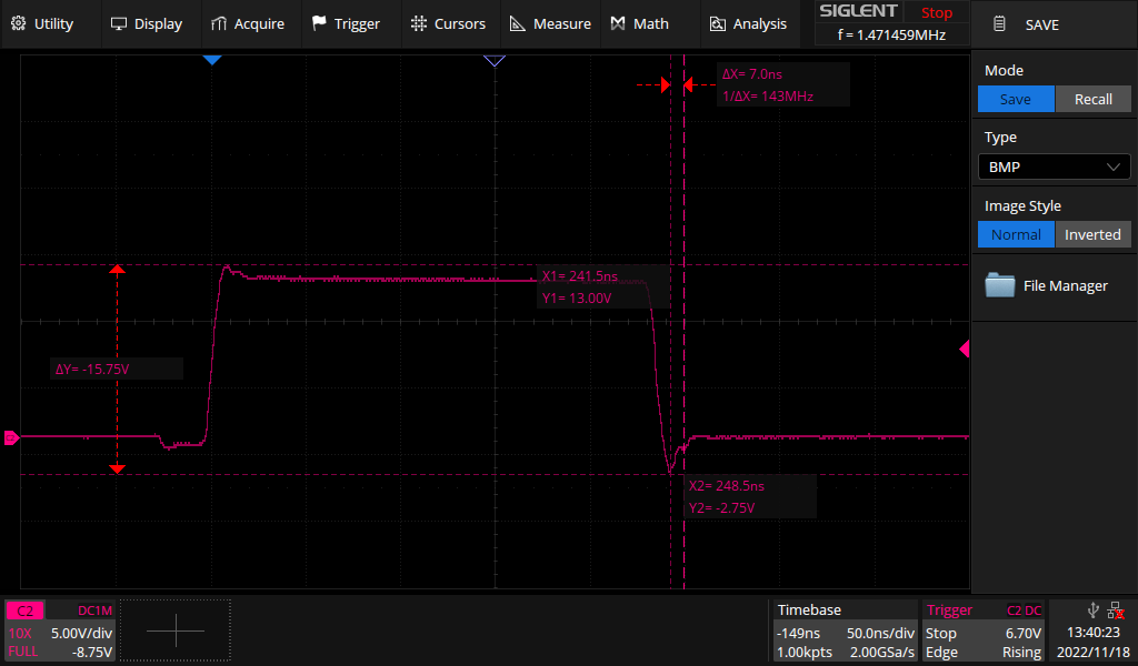
    2x RC snubber with 2R resistor and 1nF capacitor. One snubber between SW node and GND (Low Side) , and the other between SW and VBUS (High Side):

    5V in;

    Unfortunately i don't have a piccture of it, but the result is pretty much the same as with 12V in.

    12V in:


    The low side snubber did not change the SW significantly, but the high side lowered the low voltage from -4.25V (outside absolute maximum value, (AMV) ) to -2.75V (still outside AMV).

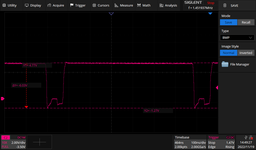
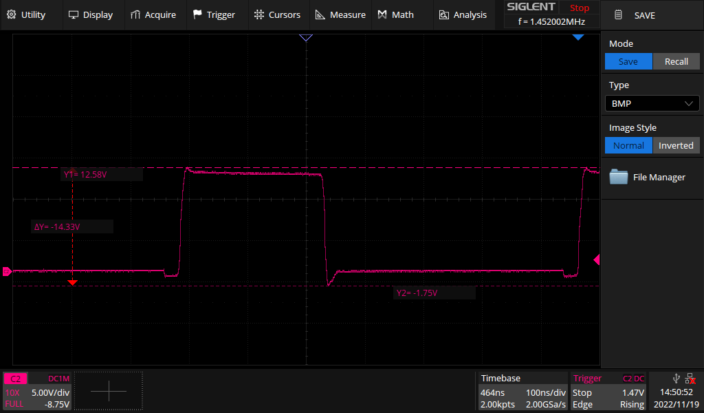
    Changed the High Side snubber to 10R and 1nF:

    5V in:

    12V in:

    Result: Reduced the low voltage to -1.27V @ 5V in and to -1.75V @ 12V in.

    I also looked at the spectrum for this snubber and compared it to the spectrum without snubber (both with 12V in):

    Without snubber:

    with snubber:

    We can cleary see that at the high end of the spectrum have significantly been reduced. The low end of spectrum has also been reduced, perhaps not as much as in the high end. 

    The ~1.5 MHz spike is still present:

    Is there any way we can reduce the ~1.5 MHz spike as it seems to be the root cause?

    Regards, 

    Sindre

  • Hi Sindre,

    You can also try adding a resistor in series with the bootstrap capacitor to slow down the slew rate.

    Resistor values of 0Ω to 10Ω should not cause significant performance impact. Higher values will begin to impact efficiency but can also be used if necessary.

    Regards,

    James

  • James, 

    I have now added a 10R resistor on BTST. So current modification includes the following:

    • 1nF capacitor on VBUS
    • 1nF capacitor on PMID
    • 10R + 1nF snubber between SW and GND
    • 10R + 1nF snubber between SW and VBUS
    • 10R resistor on BTST

    Result (only 12V in tested this time):

    The 10R resistor on BTST did not solve it. Actually, the spectrum became slightly worse. Any other suggestions? Other than 1nF capacitor on SYS and BAT as stated in the document I linked to earlier?

    I would really try to minimize the ~1.5 MHz spike if that is possible. 

    Regards, 

    Sindre

  • Hi Sindre,

    We are still looking into this. I will provide an update in the next two business days.

    Regards,

    James

  • Hi Sindre,

    Reducing the 1.5MHz spike specifically will be very difficult since this is the switching frequency of the charger. Also, if both parts of your system use BQ25890 switching at 1.5MHz, but only one part shows the unwanted EMI, then the issue may come from another source.

    Based on your original graph showing the frequencies above the FCC EMI standard, it looks like the snubber solution would have reduced the EMI peaks below the target threshold. Are you still above the EMI standard target after the snubber implementation (before the bootstrap resistor)? Our EMI solutions are targeted for meeting this standard but pushing the EMI even lower would require more complex external design.

    Regards,

    James

  • Hi James, 

    then the issue may come from another source.

    I have used E-field and H-field probes to sniff on the board, and only the charger circuit seem to be the culprit. I was thinking that the layout was part of the problem in part 1 since there is difference relative to part 2. Part 1 and part 2 also have completly different form factors, and part 2 have a display nearby the charger circuit which may act as a shield. This may be the reason for part 2 passes.

    I will ship the modified unit to test lab now and hope for the best. There is one other solution. We do not sell wall adapter with our product so i can try to find one that is better. We have seen that different adapters gives different results, but so far all have been above the limit. 

    Are you still above the EMI standard target after the snubber implementation

    I can not replicate the compliance test lab setup here so i have made relative measurement. I used the faulty unit as baseline and with the snubber it seems that the emission is a few dBs lower. And taken the original graph the few dB will probably get us below the limit, but with a low margin.

    I was thinking about putting an EMI pi-filter on the input of the charger, but that will only help for conducted measurements, and we do not have an issue there. 

    Shielding box is also another solution, but really difficult to implement at this point in time as we are soon to go into mass production and it will require a huge change in layout.  

    Thank you for all your input. 

    Regards,

    Sindre

  • Hi Sindre,

    My pleasure! If you have any other questions let us know here on E2E. For now I will mark this thread as closed.

    Regards,

    James