This thread has been locked.

If you have a related question, please click the "Ask a related question" button in the top right corner. The newly created question will be automatically linked to this question.

LM5127-Q1: Sleep Mode for Boost

Part Number: LM5127-Q1


Hello,

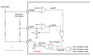
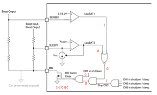
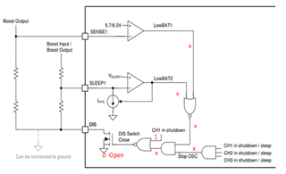
There is Sleep Mode for VOUT1 when it is configured as boost. This is explained in the pin description in p.5 of the datasheet as "When CH1 is configured as a boost, it is allowed to enter sleep mode when SLEEP1 is greater than 1.0 V". What senario is expected here? In what situation SLEEP is greater than 1.0V and less than 1.0V?

Thank you.

Regrads,

Oguri (TIJ automotive FAE)

  • Hi Oguri,

    this is selected by pin SLEEP1 and depending on the voltage applied here the mode is selected. The threshold level of this signal is 1V.

    Typically, this is set with a voltage divider between car battery and GND - see 8.2 Func block diagram

    Best regards,

     Stefan

  • Hi Stefan,

    Thanks you. But what I would like to know is in what situation this feature is good. I cannot understan how this feature can be an advantage for the circuit designer. How can the circuit designer use it? What purpose is it for?

    Regards,

    Oguri

  • Hi Oguri,

    please have a look at Figure 8-27. Deep Sleep when CH1 = Boost

    I think this explains it very well. If SLEEP1 is below the defined level (set by the resistor divider) then and all sleep requests are there, then the Sensing Resistor divider can be disabled to avoid a continuous discharge current. This will highly enhance the battery standby time.

    Best regards,

     Stefan

  • Hi Stefan,

    I am afraid, what I would like to know cannot be found in the datasheet. And please remember, Deep Sleep is activated when SLEEP1 is greater than 1.0V.

    I would like to change the question. The new question or request is an explanation for how the EVM is designed. On the EVM the resistor divider for SLEEP1 consists of 100k and 14.3k, which sets the threshold at 8.0V. But when VIN is at 8.0V it should be well in the Bypass Mode, because VOUT1 target is 6.9V. I guess the device would never enter Deep Sleep. Or Deep Sleep is activated and still meaningful even in Bypass mode? Would you please explain why the EVM is designed so?

    Thank you.

    Regards,

    Oguri

  • Hi Oguri,

    I will double check with the expert on this device. 

    He will be back in the office next week.

    Best regards,

     Stefan

  • Hi Oguri,

    here comes a detailed description about the SLEEP feature in the LM5127

    But below is my understanding of why it is important

    • SLEEP and SENSE pin pin can be used to disconnect the boost channel (CH1) feedback resistors
    • This helps lower the IQ when all channels are in sleep mode
      • happens if all three channels are in sleep.
    • A lot of the benefit comes in the pre-boost + 2 post buck configuration
      • This is typically for application that operate in skip mode and want to keep the IQ as low as possible at light loads.
      • In this case removing resistor dividers will help reduce the system level IQ.
    • Note  DIS pin does not have to be used, it is intended to help lower the IQ if required.

    Below is a summary of all the common cases of operation.

    Assuming all the buck channels are in sleep and Channel 1 (boost channel) is enabled.

    Channel 1 enabled

    SLEEP1 < VSLEEP1

    SLEEP1 > VSLEEP1

    SENSE 1 <5.7V

    Awake and ready to regulate

    Awake and ready to regulate

    SENSE1 > 6.0V

    Awake and ready to regulate

    Disonnected for the lowest IQ possible.

    • Basic idea is that the only time the disconnect pin is open is when the boost channel doesn’t need to regulate
      • The boost will be operating in bypass mode
      • This will lower the IQ of the system by lowering the current pulled by the feedback resistors
    • The SENSE pin is a fixed voltage that says the boost channel needs to wake up and get ready to switch
    • The SLEEP pin is configurable.
    • In an example the user might want to regulate the output voltage at 7V
      • SLEEP threshold should be set above this to make sure the device wakes up. I would set it around 8V to allow time for the device to wake up and be ready to regulate
    • Note if one of the buck channels (2 or 3) wakes up the disconnect will be closed and pull some IQ
      • This is regarding my comment below. The buck converters must operate at really low current to get all the channels to operate in sleep.

    If Channel 1 is disabled, the DIS pin is always open to help lower IQ

    Hope that answers your question. In summary it is to help lower the IQ.

    Best regards,

     Stefan

  • Hi Stefan,

    Thank you very much for the exhaustive discussion. Now I understand it well.

    Thank you.

    Regards,

    Oguri

  • I would like to add a recap of the discussion here:

    SLEEP1, or Deep Sleep Mode, is to reduce the quiescent current by disconnecting FB resistors when both BUCK1 and BUCK2 are in Sleep Mode and VBAT (battery voltage) is high enough not to boost it. Boost is only necessary when VBAT is lower than some specific voltage, which is slightly higher than the boost target voltage. So, FB for boost may not always be active when VBAT is high enough. If for example nomial VBAT is 13.5V while boost target is 8V, boost is only necessary when VBAT is lower than, say 9V maybe. With the voltage divider at SLEEP1 designed at, for example, 10V for the device to enter Deep Sleep, you can save the current through FB registers flowing through them by disconnecting them.

  • Hi Oguri,

    thanks for the recap.

    Best regards,

     Stefan