This thread has been locked.

If you have a related question, please click the "Ask a related question" button in the top right corner. The newly created question will be automatically linked to this question.

TPS4811-Q1: MOSFET turn on timing control

Part Number: TPS4811-Q1

Hi Team,

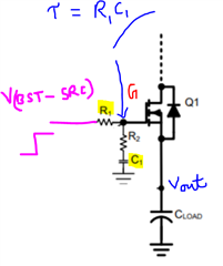
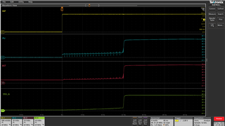
I'd like to following the previous thread, I can turn on the MOSFET after change the Rg to 100KOhm. But, the trun on timing 350ms is too slow for our application.

so I trying to change the Rg(R371) to 51KOhm, the trun on timing decrease to 200ms. But, still can not meet design requirement. 

Then I remove the R1207 and keep the R371 as 51KOhm, the turn on timing decrase singnificant around 12ms. 

Have some questions.

1. Why MOSFET cannot be turn on when R371=0Ohm

2. I couldn't fine the current path of R1207/C305 during the gate charge. Is IC inside connect SRC and GND pin? 

3. How to calculate the turn on time with Rg/CBST/MOSFET Ciss?

Thank you

Muhsiu

  • Hi Muhsiu,

    For R371=0Ohm, the dv/dt of output will be high causing to trigger short-circuit protection. 

    What is your target turn-on time? why it is important ?

    What is your application?

    Can you live with out Cout  in your application ?

    Can you share your system requirements like below to suggest the solution

    Best Regards,

    Rakesh

  • Hi Rakesh,

    Basically, I want turn on time as fast as possible, but due to the inrush current during the turn on transient. The Ids have to meet the MOSFET SOA. 

    Our application is kind of redundant power, The back to back FET have to turned on when either rail A or rail B loss power.  

    I'd like to the learn the principle of the TPS48111 turn on operation including how to calculate the trun on timing, How to select Rg etc,.

    Thanks,

    Muhsiu

  • Hi Muhsiu,

    Thanks for sharing the use case

    Sorry few more questions

    What is the Cout ? What is the target switch over time from rail-A to rail-B ?

    What is the EE ?

    Best Regards,

    Rakesh

  • Hi Rakesh,

    Both of rails Cout around 210uF. I expect less than 10ms for switch over time. 

    thanks. 

    Muhsiu

  • Hi Muhsiu,

    Following I = C* dV/dt we get I =  210uF *54V / 10ms = 1.134 A is the target inrush

    Equation 3 can be used to compute required C1 value for a target inrush current. A 100 kΩ resistor for R1 can be a good starting point for calculations.

    Use a damping resistor R2 (~ 10 Ω) in series with C1.

    So, for your design

    R1 = 100 kΩ 

    R2 = 10 Ω 

    we get C1 as 15nF

    Best Regards,

    Rakesh

  • Hi Rakesh,

    Is back to back topology still can use this method?

    I couldn't fine the current path return to ground of R2/C1 during the gate charge. Is IC inside connect SRC and GND pin?

    I use R1=100KOhm, without install R2/C1 to do experiment before, turn on time is around 350ms. 

    Thanks,

    Muhsiu 

  • Hi Muhsiu,

    Is back to back topology still can use this method?

    Yes

    I couldn't fine the current path return to ground of R2/C1 during the gate charge. Is IC inside connect SRC and GND pin?

    The dv/dt control is with reference to GATE. Having R2/C1 diverts the GATE charging current and slows the GATE dv/dt rate to limit the inrush current.

  • Hi Rakesh,

    This is  FAE support Musiu for this case in field and customer would like to know whether you could provide the formula Vgs of Q1 which should be related R1, Q1gs, Ipu , R2, C1. 

    They would like to know the rising time of Vpu as below figure is reasonable. Thanks.  

    Regards,

    Ben

  • Hi Ben,

    V(BST-SRC) is the voltage appears at the PU pin, which charges the GATE VG of Q1 with a time constant of R1C1. As it is a slow ramp-up, the MOSFET Q1 works as source follower with Vout = VG - Vgs_Q1

    The timing is decided by the equations (2) and (3)

    Best Regards,

    Rakesh