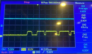
We have efficiency and unstable output issue. We did not change anything in the LM5176EVM schematic except input capacitance. We designed 4 layered board. The output is stable with no load and switching signals are fine in both modes. But in boost mode the voltage output is unstable and the signals (SW1, SW2, HO1, LO1, HO2, LO2) are abnormal and the board could not even provide stable output @1A load. The buck mode output is more stable than boost mode but the efficiency falls to 76%. Also, the buck-boost mode is not stable @2A load
Requirement:
Vin: 6 to 36V; Vout: 12V/10A or 18V/4A; fsw = 250kHz; expected efficiency @4A load - more than 90%
1. Could you check the layout privately?
2. Is it possible to deal with noise without changing 4 to 6-layered PCB?
3. How to improve efficiency?
We tried the following steps but failed:
- Compensation element update using LM5176 Quick start tool @CCM mode.
- Slope and SS capacitor update
- disabled Hiccup and DITHering mode.
- Tried at the different switching frequencies
- Built and checked with the new board but the same result
- Replaced MOSFETs and IC
- The elements did not hot at all when the load is connected
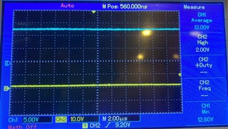
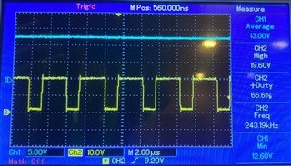
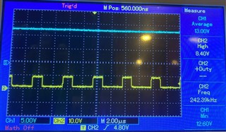
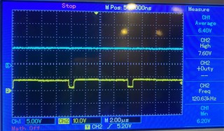
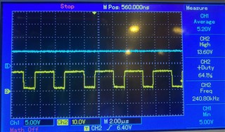
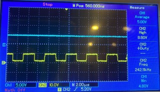
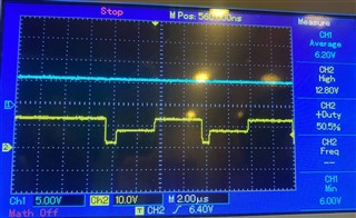
Attached boost mode switching signal.
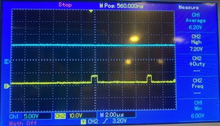
CH1 - VOUT 12V; CH2-SW1 @No load
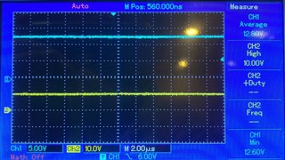
CH1 - VOUT 12V; CH2-SW2 @No load
CH1 - VOUT 12V; CH2-HO1 @No load
CH1 - VOUT 12V; CH2-LO1 @No load
CH1 - VOUT 12V; CH2-HO2 @No load
CH1 - VOUT 12V; CH2-LO2 @No load
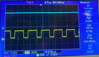
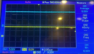
CH1 - VOUT 12V; CH2-SW1 @14W load
CH1 - VOUT 12V; CH2-SW2 @14W load
CH1 - VOUT 12V; CH2-HO1 @14W load
CH1 - VOUT 12V; CH2-LO1 @14W load
CH1 - VOUT 12V; CH2-HO2 @14W load
CH1 - VOUT 12V; CH2-LO2 @14W load