This thread has been locked.

If you have a related question, please click the "Ask a related question" button in the top right corner. The newly created question will be automatically linked to this question.

LM5113-Q1: Gate driver for GaN-based Class-D audio amplidier

Part Number: LM5113-Q1
Other Parts Discussed in Thread: LM5113

Dear,


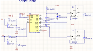
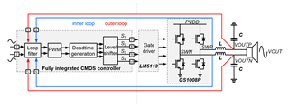
We chose LM5113 as the gate driver for GS1008P in our class-d audio amplifier (CDA), and there's a phenomenon we can't explain. We think the gate driver may cause it. Our CDA is an H-bridge structure, and the switching frequency is 1.8MHz.

The supply voltage is 50V, and the load resistance is 4Ω. A system-level circuit is attached. 

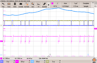
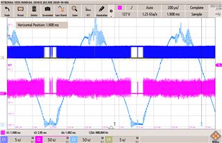
 (For the attached waveforms, C1 is SL, C2 is SWP, C3 is VOUTP, C4 is SH.)

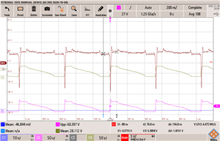
When the input of the CDA exceeds the limit (Pout=200W), the output will be clipped, that is, the top and bottom of the output waveform will be flattened symmetrically.

However, our test results (VOUTP) show asymmetry. More specifically, the lower switch of a half-bridge can be normally open for a long time when clipping, but the upper switch cannot.

We want to know whether the upper and lower paths of the LM5113 are asymmetric, or what other reasons are.

Best regards

Minggang

  • Hi Minggang,

    There is a limit for how long the high side can be ON. For the high side to be on, it has to draw power from the bootstrap capacitor. I think that maybe the bootstrap capacitor isn't large enough. See section 8.2.2.2 in the datasheet for sizing the bootstrap capacitor.

    Can you take a scope shot of pin HB? This will tell us if the capacitor is losing too much voltage.

    Keep in mind that normally increasing the size of the bootstrap capacitor also requires increasing the size of the VDD bypass capacitor.

    Best Regards,
    Ethan Galloway

  • Hi Ethan Galloway,

    We use a 1uF bootstrap capacitor, and the limit of the high side may be more than 1ms.

    The attachment is the zoom-in of the previous attachment.

    Best regards

    Minggang

  • Hi Minggang,

    1 ms is pretty long for the high side. Keep in mind the GS61008P has 200 uA gate to source current which is larger than a normal silicon MOSFET. You can use the equation I = C dv/dt to determine the total voltage drop caused by the GS61008P gate to source current after being ON for 1 ms.

    Do you know what the longest high side ON time that you are expecting is?

    Please let me know when you have a scope shot of the bootstrap capacitor.

    Best Regards,
    Ethan Galloway

  • Hi Ethan Galloway,

    The high side and low side should be symmetrical, the longest on-time of the low side is 100us~200us.

    The longest high side ON time that we expect is 100us~200us, which is much less than 1ms.

    But the high side keeps switching, and the actual longest on-time is 1us~2us.

    For LM5113, are the high and low sides symmetrical in circuit design?

    Best regards

    Minggang

  • Hi Minggang,

    Yes, the high side and low side have symmetrical drivers. The only difference between the high side and the low side is that the high side is powered by the boot strap capacitor through pin HB. You can see that the high side and low side are the same in the block diagram here, but that the high side and low side are powered differently.

    Best Regards,
    Ethan Galloway

  • Hi Ethan Galloway,

    Can you explain the asymmetry in our test? We couldn't find the reason.

    Best regards

    Minggang

  • Hi Minggang,

    There could be multiple reasons for asymmetry. The high side is powered from the bootstrap capacitor. If VHB falls below 3.2 V, the high side enters into UVLO. UVLO mode disables the high side driver. I think your part is entering into UVLO for the boot strap capacitor.

    Another cause for asymmetry is the clamp on the high side to prevent the bootstrap capacitor from overcharging. I don't think this is your problem though.

    Can you measure the voltage between HB and HS on the oscilloscope? This will tell us whether or not the high side is entering into UVLO and the capacitor is running out of energy.

    Best Regards,
    Ethan Galloway

  • Hi Ethan Galloway,

    For a  1uF bootstrap capacitor, I think 1us~2us on-time for the high side is very short, it can't enter into UVLO.

    Maybe other reasons happen for this asymmetry.

    The attachment is the half schematic of the gate driver and GaN.

    Best regards

    Minggang

  • Hi Menggang,

    I'll talk to my coworkers to see if there is any other causes.

    To recap, you need to make both the high and low side symmetrical?

    I help make the low side and high side symmetrical, but I'll need some more data first. Could you take a oscilloscope picture of the inputs and the bootstrap capacitor? For the bootstrap capacitor, measure HB to HS.

    Also, is your scope shot of the high side output measuring HO to HS?

    Best Regards,
    Ethan Galloway

  • Hi Ethan Galloway,

    Yes, we need both the high and low sides symmetrical.

    I will check HB to HS later.

    I didn't measure HO to HS, I just measured the input of LM5113 and SWP to see if the GaNs work well. 

    Best regards

    Minggang

  • Hi Minggang,

    Thanks. I'll help with obtaining symmetry,

    Let me know when you have those measurements.

    Best Regards,
    Ethan Galloway

  • Hi Ethan Galloway,

    I have got the waveform of the bootstrap capacitor, please check the attachment.

    M3 is the voltage of bootstrap capacitor, it keeps at about 5V.

    Since we don't have a differential probe, we use the math of the oscilloscope.

    Because the glitch is too large, the average mode is chosen. 

    Best regards

    Minggang

  • Hi Minggang,

    The capacitor voltage drops nearly a whole volt which isn't good. I would recommend bumping up the bootstrap capacitor. Keep in mind that the driver and GaN FET performance is heavily based off of the voltage supply. The high side needs to have between VHS+4 and VHS+5.5 supplying it.

    Also keep in mind that for a class D audio application, the bootstrap capacitor may very little time to charge back up again if the duty cycle of HO is very high.

    Can you image HO to HS?

    Best Regards,
    Ethan Galloway

  • Hi Ethan Galloway, 

    The capacitor voltage didn't drop that large (the large glitch), and the waveform is caused by inaccurate measurement.

    We just focus on the dc of the voltage, and it keeps between 4V and 5V.

    And thank you for the useful suggestions, we will keep you update.

    Best regards

    Minggang

  • Hi Minggang,

    I know the big downwards spike in the math function is a glitch. I was referring to the smaller drops after the initial peak.

    If you want a more symmetrical waveform, you will have to have a more stable bootstrap capacitor voltage. The performance of the high side is dependent on the bootstrap capacitor voltage.

    One more thing, it looks like your capacitor charging circuit gets power from HS to charge VHB? We normally recommend that D2 should connect VDD to VHB through a 100 ohm resistor. This circuit is responsible for providing power to the high side circuit.

    Best Regards,
    Ethan Galloway

  • ok, thank you!

    Best regards

    Minggang

  • Hi Minggang

    I took another look at your setup. With your current circuit, the bootstrap capacitor will start being drained when the high side turns on. Transistor Q1 will form a path for the capacitor to drain at about 0.2 mA.

    I would recommend using the recommended setup in the datasheet for best performance. Using a zener diode to charge the capacitor and as a clamp is pretty creative and I've never seen that done before.

    Best Regards,
    Ethan Galloway