This thread has been locked.

If you have a related question, please click the "Ask a related question" button in the top right corner. The newly created question will be automatically linked to this question.

UCC28180: Question about UC28180 starting to work and the loop compensation formula

Part Number: UCC28180


Dear Mr. TI
Hello, I have a question about UCC28180.

Q1. How to start generating PWM signal?
 Suppose there is no current flowing in Rsense at first.
 That is, Isense = 0.
 Then the -2.5x Amp output is also 0v.
 Since the gmi amp has 0v input, the output current is 0A.
 Then the ICOMP voltage is 0v, so ICOMPP = 1, and by OR4, FAULT = 1.
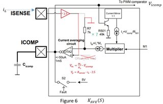
 The bottom right SW turns on by FAULT
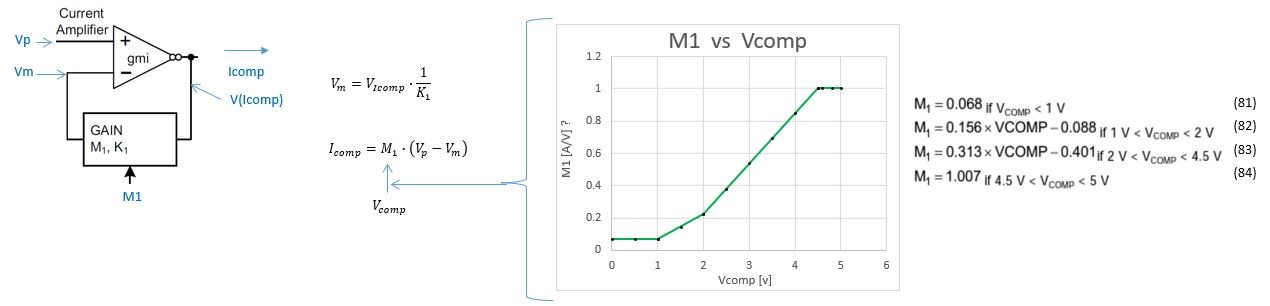
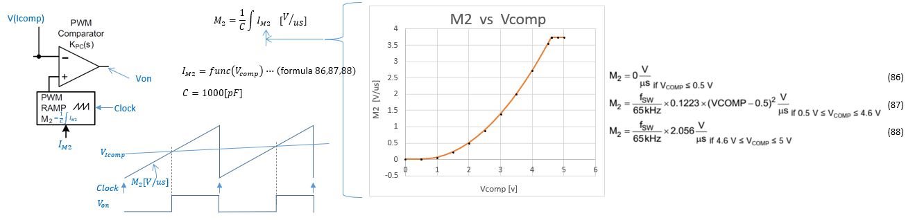
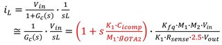
 When VCOMP = 0v, M1 = 0.068x and M2 = 0[v/us] for the M1M2 generator circuit.
 Since the gmi input is still at 0v, ICOMP=0.068*0v[A], and I don't think ICOMPP will be released anytime soon.
 Please let us know if there is any error.

Q2. Regarding the M1 and M2 generation circuits
 In equation 78 on page 30, the product of M1 and M2 is related to Iout, Vout, Vin, and switching frequency.
 On the other hand, in equations 81 to 84 on page 31, M1 is expressed as a function of Vcomp.
 Also, in equations 86 through 88, M2 is also expressed as a function of Vcomp.
 By the way, Vcomp is generated when the error amplifier adds or subtracts the VCOMP voltage from or subtracts from the target value using the gmv amplifier with respect to the point where the error amplifier is balanced with 5v.
Vcomp is generated by adding or subtracting the Vcomp voltage from or from the target value with the gmv amplifier.
From this flow, I feel that Vcomp voltage is not directly related to Iout, Vout, Vin and switching frequency.
Please let me know what you mean by equation 78.
Please do so.
Thank you for your support.

  • Hi,

    Thank you for the query on UCC28180.

    On your first question, you are correct, this is one of the protection features of UCC28180 where ICOMPP (COMP open pin protection), whenever ICOMP falls below 0.2V the PWM switching will be halted and is documented in the datasheet.

    On your second question, Vcomp is related to M1M2 (which in turn depends on Iout/Vout/Fsw etc.) as against your claim. You can download the excel calulator for UCC28180 and this shows hows they are related in the sheet titled "VCOMP".

    Regards,

    Harish

  • Hi, Harish-san

    Thank you for your prompt reply.

    Thank you for the sluc506c.xls.

    I have confirmed that the M1M2 equation is contained in cell "H7" of the "VCOMP" sheet.

    Q3. 78 Derivation of equation and VCOMP  relationship

     What I would like to know is the derivation of the M1M2 equation and the VCOMP equation.

    Please let me know if you have any good references.

    By the way, I have read all the datasheets of UCC28180 and understand everything except the part related to compensation such as M1M2.

    I have also read and understand SLYY131 ( www.ti.com/.../slyy131.pdf ).

    By Robert W. Erickson and Dragan Maksimovic, fmipa.umri.ac.id/.../R._Erickson_Fundamentals_of_Power_ Electronics_pBookZZ.org_.pdf

    I have also read and closely read the relevant sections.

    Q4. About the value of M1 and M2 and the circuit

     We believe the following.

    Please point out any errors.

    Q5. isn't the following a misprint?

    9.2.2.9 Sense Resistor To accommodate the gain of the non-linear power limit, the sense resistor, RSENSE,  is sized such that it triggers the soft over current at 10% higher  than the maximum peak inductor current using the minimum soft over current threshold of  the ISENSE pin, VSOC, of ISENSE equal to 0.265 V.

     I see "0.265V", but isn't the correct answer 0.285Vtyp?

    And am I correct in my understanding that the actual calculation (equation 51) uses 0.259Vmin?

    9.2.2.10 Output Capacitor

    Equation (60) is defined in terms of ripple, so it must be doubled?

    Q6. Confirmation of erroneous information in another document

    www.ti.com/.../slyy131.pdf

    Page 11:  2 Phase, ICout_rms Calculation Outline

    Page 15:  Substitutions

    Page 20:  References

    By the way.

    fmipa.umri.ac.id/.../R._Erickson_Fundamentals_of_Power_Electronics_pBookZZ.org_.pdf

    Page 1378:  Integration of powers of sinθ over complete half-cycle

    This is incorrect at this literature point.

    Thank you for your support.

    Miyauchi

  • Hi Miyauchi-San,

    Thank you for the query.

    I will check the equation and get back to you in a couple of days.

    Regards,

    Harish

  • Thank you for your  thoughtful message.

    Miyauchi

  • Hi Miyauchi-San,

    Please find my reply pointwise below:

    For Q3 & Q4 please refer the attached document equation 14. This clearly shows derivation of equation 78 and table - 1 presents the details of non linear M1M2 block along with equations 20-24.

     PFC_document.docx

    Q5. Yes, 0.259 is used for calculation for sense resistor. Also the datasheet mentions 0.285V, pleas refer figure 16 or datasheet section on system protection with VSOC. You need not double the output ripple voltage, because it already considers the second harmonic pk-pk line voltage ripple so the datasheet equations are correct.

    Q6. For this question, honestly I haven't hand derived these and I would suggest you verify through simulations to cross your results to see if there is any issue with the formula.

    Thank you 

    Regards,

    Harish

  • Hi, Harish-san

    Thank you for your prompt reply.

    Thank you for sending us the M1M2 explanatory material.

    I will read them carefully from now on.

    I received your email at 8:49 pm. Does that mean it was sent at 5:49 am local time?

    Thank you for your response so early in the morning. Please take your time to answer next time.

    Thank you very much for your cooperation.

    Best regards,

    Miyauchi

    P.S.  The World Cup is being held.  We are cheering for the U.S. as well.

  • Hi Miyauchi-San,

    Thank you for the reply. Please let us know if you have any questions.

    Regards,

    Harish

  • Hi, Harish-san

    Thank you for your prompt reply.

    Thank you for sending me the PFC_document.docx.

    I understand most of it now.

    I have a few questions and confirmations.

    Q1.  4.1.1 ΔVout/ΔIout

    [ A few algebraic manipulations would show that the shunt resistor Re always equals the DC load resistance

     Rout, thus it changes depending on the power delivered by the system. ]

    From Figure10 Power stage modeling, we can formulate the equation dVout/dIout as

    Therefore, we know that the equations for Resistive Road and Constant Power Load can be obtained by setting Re=+Rout and Re=-Rout, respectively.

    Then I would like to ask why Re=+Rout and Re=-Rout.

    What we are imagining here is that the Output Stage model is equivalent to

    Think of a constant current source and an adjustable resistor Re, and in the case of Resistive Road, the system controls the internal Re to adjust to the load Rout by Re=+Rout, and

    In the case of Constant Power Load, is it correct to understand that it is equivalent to say that the system controls the internal Re to adjust Re=-Rout with respect to the load Rout?

    Q2. 4.2 Small signal transfer function of ΔVout/Δ(M1M2) for voltage loop analys

    I understood up to equation 23.

    By the way, in equation 107 of datasheet UCC28180, I see M3 and 1v.

    Is M3 referring to Gnon or 1v referring to the input signal voltage for gain calculation?

    Actually, I am building a SPice-Lib and want to model the circuit.

    If M3 exists, I need to add that to the model as well.

    Please let me know.

    Q3.  Check for errors        Figure 6 K_AVE (S)

    Is there an error and is the correction in red correct?

    Q4. 3.4.Open loop transfer function gain for current loop

    Is the denominator in Equation 13 a misnomer for the numerator?

    The equation shows that

    Q5. 4.2. Small signal transfer function of ΔVout/Δ(M1M2) for voltage loop analys

    [ then the transfer function of dVout/dVcomp ]

    →then the transfer function of dVout/d(M1M2)

    is correct?

    Q6.  Rationale for previous question(2022/11/21)

    www.ti.com/.../slyy131.pdf

    page20

    The correct answer can be derived as follows, I think.

    By the way, I think the 4 cubic equation is correct.

    OKBangbang

    Please check it.

    Regards;

    Miyauchi

  • Hi Miyauchi-San,

    Thank you for the query again.

    At this point I do not have much answers to your querries as your concerns require deriving equations and I might need to consult with the product definers of this IC for some of your querries. I will keep ou updated.

    Regards,

    Harish

  • Hello Miyauchi-san, 

    Harish is out-of-office for a few days.  I will try to answer your latest questions from Dec 14th, above.

    Q1:  Regarding Re = +/-Rout, I believe that your understanding is correct. Re is negative in the case of a constant power load, since the slope of Vo/Io is negative (if Vo goes down across the constant power load, Io goes up).

    Q2:  Yes, I believe that M3 corresponds to Gnon of the "PFC Document", and M3 is the slope (or derivative ) of M1*M2.  I think that the 1V term is simply a factor added to cancel an additional "V" unit introduced by M3, to keep the resulting gain of Gpwm_ps(f) unit-less. 

    Q3:  Since the "PFC_Document" comes from an Infineon document for ICE1PCS01, I'm sure that Figure 6 is correct for their device.  It is likely that the modifications you drew on the Figure are applicable to the the UCC28180.  

    Q4:  I believe that equation 13 is correct, since it is used later for further gain derivation.  The additional factor 2.5 does apply with the UCC28180. 

    Q5:  Yes, I think the paper derives G23(s) only from Δ(M1M2) to ΔVout.  There is probably more to the paper that later includes Gnon, but is not shown in the excerpt presented in "PFC Document".   Adding Gnon(s) would eventually lead to the transfer function of dVout/dVcomp.

    Q6:  I am not in a position to contest your derivation of the 6-cubic equation.  I'll take your word for the correct result. :-)

    Regards,
    Ulrich

  • Hi, Ulrich-san, Cc Harish-san

    Thank you very much for your quick and courteous replies.

    I would like to inquire about some points that are unclear.

    Q1: I know by feel that Re is likely to be positive or negative.

    Then it would be very helpful if you could derive why exactly the values are Re = +Rout or Re = -Rout.

    (Actually, I understand the polarity, but I don't understand why the value of Re is the way it is.)

    Q2: My goal is to create a Spice-Lib.

    Ignoring M3 in the 107 equation in datasheet UCC28180 because it is unknown, I formed M1 and M2 according to your reference and ran Spice, and it works as expected with PFC.

    Then what is M3 and what does M3 in the datasheet's 107 equation represent?

    The question is.

    M1=f1(Vcomp) from equations (81)-(84)

    M2 = f2(Vcomp) is obtained from equations (86) to (88).

    Then, what is M3?

    Q3: I see that this was an Infenion literature.

    I have looked for it but cannot find it.

    Could you please contact me with the website of the literature?

    I will read it carefully.

    Q4: Equation (11) shows an open-loop transfer function.

    Since we derive it as closed-loop from equation (12)

    Equation (13) does not agree with equation (11).

    The numerator of equation (13) is the reciprocal of the numerator of equation (11). Naturally, the denominator of equation (13) should also move to the numerator side of equation (11).

    ...Since equation 103 in the datasheet is consistent with equation 11 in this document, equation 103 is the open-loop transfer function of the current, right?

    Therefore, I think the denominator of equation 13 is incorrect.

    Q7: Figure 5 current loop block diagram is understood.I think this is the same as G2 of Figure 8 Large signal modeling of voltage loop or Figure 9 Small signal modeling of voltage loop,  However, Block diagram is different.

    Please let me know.

    Regards,

    Miyauchi.

    ┗|´・_●・|┛Merry  Christmas!

  • Hi Miyauchi-San,

    Thank you for the query on UCC28180.

    Q1. On the mathematical derivation of emulation resistor Re, I see the concept is introduced in Robert ericksson book as Loss Free Resistor (LFE) model and I also happended to find the following paper where they have used small signal modelling and partial differention to derive the expressions. Report-Mingyao_Gong.pdf

    Please refer to pages 30-35 in the above link.

    Q2. I think M3 is basically a correction term to ensure the M1M2 product is satisfied as shown in the datasheet example M3 of 1.003 is used to balance the gains of 0.747 and 0.751V/us

    Q3. To be honest we do not have any access / material similar to the infineon document discussed above. I am not sure if we can offer more help here or with respect to spice lib file creation.

    Q4. I think both the equations, i.e 103, 11 and 13 mentioned are correct. Equation 103 mentions transfer function with Vout and L and hence we have the s^2 term in the denominator, whereas equation 13 of the document mentions in terms of Vin and Vout and hence the 'sL' terms cancel out. So both are consistent for me.

    Q7. Yes figures 5 and 8 are consistent , but to get to figure 9 you might need to perform a perturbation and linearization of the model in figure 8 to get to figure 9 and you will get the missing terms.

    Regards,

    Harish

  • Hello Miyauchi-san,

    As I mentioned in my answer to Q2, above, M3 is the derivative (the slope) of the product of M1*M2.  It corresponds to the factor "Gnon" in the paper.  
    Here is the version of the full paper that I have, from 2007.  ANP0013-v1.3_Control_Loop_Modeling.pdf 
    There may be a later version on the web, but I don't know about that. 

    Regards,
    Ulrich

  • Hi,  Harish-san, Ulrich-san

    Thank you very much for all the materials.

    I will read them carefully.

    Wishing you a happy Christmas and a glorious New Year ! .

    Regards,

    Miyauchi.

  • Hi Miyauchi-San

    Please let us know if you have further questions.

    Wishing you a merry Christmas and a happy New year 2023 too.

    Regards,

    Harish