This thread has been locked.

If you have a related question, please click the "Ask a related question" button in the top right corner. The newly created question will be automatically linked to this question.

BQ27220: How to set external thermistor

Part Number: BQ27220
Other Parts Discussed in Thread: BQSTUDIO

Hi experts,

My customer would like to use BQ27220 with an external thermistor. However it doesn't go well. Could you please answer questions below?

[Situation]

(1) Measured digital value is about 2970.

(2) When the BIN pull-up resistor was changed from 1.8MΩ to 10kΩ, the analog voltage changed, but the digital value sent to the microcontroller hardly changed.

(3) The customer think the thermistor inside BQ27220 is enabled and the external thermistor isn't enabled from the result of (2).

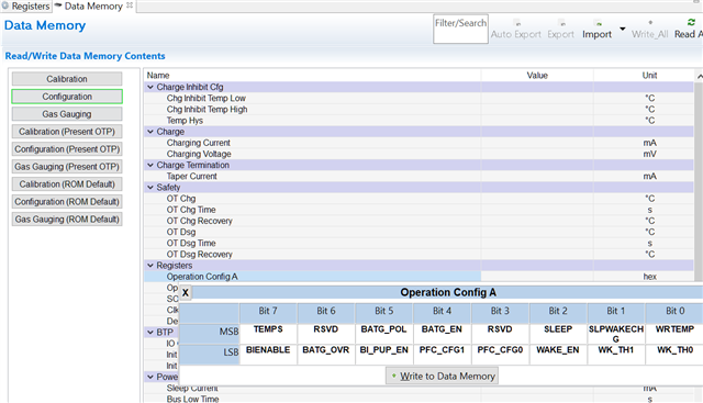
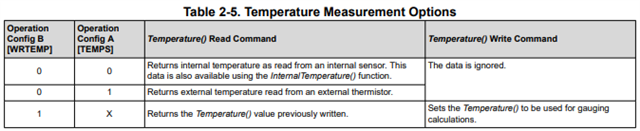
(4) The Technical Reference Manual (figure below) says that it is possible to measure temperature with an external thermistor by changing the value of Operation Config A.

[Questions]

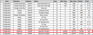
(1) I can't find the description about the address of Operation Config A. I don't know how to change the value, so could you please let me know?

(2) As a pull-up resistor for BIN, they attached 1.8MΩ with reference to the data sheet and the circuit diagram of the evaluation board. Is the pull-up resistor value of 1.8MΩ correct when actually connecting an external thermistor?

Thank you for your help.

Bes Regards,

Taito Takemura

  • You can check, if the external thermistor is enabled by probing the thermistor pin on the gauge. If it's enabled, then the gauge will turn on an internal bias resistor (about 1.8kOhm) for a few ms every second during normal mode (not sleep) so the resulting voltage from the effective divider (thermistor to internal bias || external pullups) will be visible on a scope.

  • Operation Config A location in Data memory

  • Hi Dominik, Shirish,

    Thank you for your answers.

    On the customer's board, the address is specified and written directly from the MCU through I2C communication. When they specified 0x9206 described in "Technical Reference Manual", an error occurred. Is there any problem with 0x9206 as the data address? Also, if the address is 0x9206 and there is no problem, are there any other possible causes of the error?

    Best Regards,

    Taito Takemura

  • For an example of how to read/write from MCU, See TRM section 6.1 Data Memory Parameter Update Example

  • Hi Shrish,

    Thank you for your comment.

    I had the customer follow the contents of Chapter 6 of the Technical Reference Manual, but it didn't work. Could you please tell me the procedure for changing from the internal thermistor to the external thermistor?

    They are performing I2C communication according to the instructions in Chapter 6, but it seems that sometimes the communication fails without an Ack being returned. Could you tell us if there are any restrictions such as time during I2C communication?

    Thank you for your help.

    Best Regards,

    Taito Takemura

  • Hello Takemura-san,

    Please attach the log of the commands that were sent. We can check it and see if there are any issues

  • Hi Shrish,

    The command sent to BQ27220 is as follows.
    Commands are sent according to Chapter 6 of the Technical Reference Manual. The difference from Chapter 6 is the step5&6 part in the table below, they refer to the address value of "Operation Config A" on p32 of the Technical Reference Manual. "Write" often fails, and read values are not stable.


    code

    step1

    W/R

    address

    data

    W

    0x00

    0x14

    W

    0x01

    0x04

    W

    0x00

    0x72

    W

    0x01

    0x36

    step2

    W

    0x00

    0xFF

    W

    0x01

    0xFF

    W

    0x00

    0xFF

    W

    0x01

    0xFF

    step3

    W

    0x00

    0x90

    W

    0x01

    0x00

    step4

    R

    0x3B


    step5

    W

    0x3E

    0x06

    step6

    W

    0x3F

    0x92

    step7

    R

    0x60


    step8

    R

    0x61


    step9

    R

    0x40


    R

    0x41


    Thank you for your help.

    Best Regards,

    Taito Takemura

  • Step4: Need to get value and make sure bit2 is set. Repeat read until set.

    Please provide the values of the bytes that were read

  • Hi Shirish,

    I'll share their values of the bytes that were read. (step4,7,8, and 9)

    Could you please give us your comment regarding their situation?


    code

    step1

    W/R

    address

    data

    W

    0x00

    0x14

    W

    0x01

    0x04

    W

    0x00

    0x72

    W

    0x01

    0x36

    step2

    W

    0x00

    0xFF

    W

    0x01

    0xFF

    W

    0x00

    0xFF

    W

    0x01

    0xFF

    step3

    W

    0x00

    0x90

    W

    0x01

    0x00

    step4

    R

    0x3B

    0xb804

    step5

    W

    0x3E

    0x06

    step6

    W

    0x3F

    0x92

    step7

    R

    0x60

    0x2411

    step8

    R

    0x61

    0xff24

    step9

    R

    0x40

    0x3c00

    R

    0x41

    0x003c

    Thank you for your help.

    Best Regards.

    Taito Takemura

  • In Step 4, bit 2(of high byte) is not yet set. Wait a few milliseconds and read the register again until it is set.

    Update: Read only 1 byte from 0x3B for clarity. Maybe the bit is set?

    There are 16 steps in the example. You will need to complete the procedure. At the end if it, check with bqStudio if the value was updated correctly

  • Hi Shirish,

    >Update: Read only 1 byte from 0x3B for clarity. Maybe the bit is set?

    When reading only 1 byte from the address 0x3B register in step 4, it was confirmed that 0x04 was returned stably. Is it okay?

    >There are 16 steps in the example. You will need to complete the procedure

    Regarding the procedure after step 9, the Technical Reference Manual only describes when changing the Design Capacity.
    So we don't know the change command to the external thermistor after step 9.
    Could you please tell me the commands after step 9 when changing to an external thermistor?

    Thank you for your help.

    Best Regards,

    Taito Takemura

  • Hello Takemura-san,

    I would recommend that you write Design capacity to verify the procedure. Once that works you can change the address and value to write the configuration.

  • Hi Shrish,

    Could you please tell me concrete commands after step9 when changing to an external thermistor?

    Best Regards,

    Taito Takemura

  • Hi Shrish、

    Sorry for the continuous post.

    They executed the command as shown below.


    Q1. New_Checksum is calculated in step 11. Is there any mistake in the calculation formula in the red cell in the table below?

    Q2. How can they determine the success/failure of the change in the steps below? Can it be confirmed by reading a register somewhere? (I would like you to tell me how to do it outside of bqStudio)


    code

    W/R

    address

    data

    step1

    W

    0x00

    0x14

    W

    0x01

    0x04

    W

    0x00

    0x72

    W

    0x01

    0x36

    step2

    W

    0x00

    0xFF

    W

    0x01

    0xFF

    W

    0x00

    0xFF

    W

    0x01

    0xFF

    step3

    W

    0x00

    0x90

    W

    0x01

    0x00

    step4

    R

    0x3B

    0x04

    Operation_Status

    step5

    W

    0x3E

    0x06


    step6

    W

    0x3F

    0x92


    step7

    R

    0x60

    0x11

    Old_Checksum

    step8

    R

    0x61

    0x24

    Data_len

    step9

    R

    0x40

    0x00

    Old_DC_MSB

    R

    0x41

    0x3C

    Old_DC_LSB

    step10

    W

    0x40

    0x04

    W

    0x41

    0xB0

    step11

    -

    Temp=(255-Old_Chacksum-Old_DC_MSB-Old_DC_LSB) % 256


    -

    New_Checksum=255-(Temp+0x04+0xB0)%256


    step12

    W

    0x60

    New_Checksum

    step13

    W

    0x61

    Data_len

    step14

    W

    0x00

    0x92

    step15

    W

    0x01

    0x00

    step16

    W

    0x00

    0x30

    W

    0x01

    0x00

    Thank you for your help.

    Best Regards,

    Taito Takemrua

  • Hello Takemura-san,

    1. The checksum calculation is correct. But check the value that is being written. You want to OR with 0x8000 to set TEMPS bit in Operation config. 0x803C. So New_Checksum=255-(Temp+0x80+0x3C)%256

    2. Repeat till step 9 to check if the value was updated. Old value will be the new value after writing.

  • Hi Shrish,

    Thank you for your answer. Could you please let me check additional things?

    (The commands mentioned in the question below refer to the previously posted Steps 1 to 16 table)

    Q1. After executing steps 1 to 16, I executed steps 1 to 9 again, but the value read in step 9 the second time was the same as the first time. Could you please check again if there are any mistakes in the addresses and values being written/read?

    Q2. If you want to change Operation ConfigA, is the address read in step5 and step6 appropriate?

    Q3. Is the value written in step 10 correct?

    Q4.In step 11, it was pointed out to calculate with "New_Checksum=255-(Temp+0x80+0x3C)%256". However, in step 11 of "Technical Reference Manual", it is "Temp + 0x04 + 0xB0".
    I interpreted it as necessary to add the value written in step 10 to Temp. Is my understanding correct?

    Thank you for your help.

    Best Regards,

    Taito Takemura

  • Did you write 0x04B0 to Operation Config? If yes, then all your original steps are correct. The checksum includes the data that is written (Your interpretation in Q4 is correct)

    Note that TEMPS bit would still be 0 if you write 0x04B0.

    If you do not get the correct results, then i  suggest that you try to write design capacity as shown in the example and see if that works. Resetting the device will reset contents of RAM, so you can try multiple times for testing

  • Hi Shrish,

    I'll share the latest information of the results from customer's command.

    After following the steps described in Chapter 6 (Changing Design Capacity) of the BQ27220 Technical Reference Manual, they checked steps 1 to 9 again. As a result, the DC_MSB and DC_LSB read in the second step9 are the same as the first time.

    Could you please give me your opinion if there is any mistake in each command and the numerical value to be written?

    Thank you for your help.

    First


    code

    W/R

    address

    data

    step1

    W

    0x00

    0x14

    W

    0x01

    0x04

    W

    0x00

    0x72

    W

    0x01

    0x36

    step2

    W

    0x00

    0xFF

    W

    0x01

    0xFF

    W

    0x00

    0xFF

    W

    0x01

    0xFF

    step3

    W

    0x00

    0x90

    W

    0x01

    0x00

    step4

    R

    0x3B

    0x04

    Operation_Status

    step5

    W

    0x3E

    0x9F


    step6

    W

    0x3F

    0x92


    step7

    R

    0x60

    0xA1

    Old_Checksum

    step8

    R

    0x61

    0x24

    Data_len

    step9

    R

    0x40

    0x0F

    Old_DC_MSB

    R

    0x41

    0xCB

    Old_DC_LSB

    step10

    W

    0x40

    0x04

    W

    0x41

    0xB0

    step11

    -

    Temp=(255-Old_Chacksum-Old_DC_MSB-Old_DC_LSB) % 256


    -

    New_Checksum=255-(Temp+0x84+0x84)%256


    step12

    W

    0x60

    New_Checksum

    0xC7

    step13

    W

    0x61

    Data_len

    0x24

    step14

    W

    0x00

    0x91

    step15

    W

    0x01

    0x00

    step16

    W

    0x00

    0x30

    W

    0x01

    0x00


    Second


    code

    W/R

    address

    data

    step1

    W

    0x00

    0x14

    W

    0x01

    0x04

    W

    0x00

    0x72

    W

    0x01

    0x36

    step2

    W

    0x00

    0xFF

    W

    0x01

    0xFF

    W

    0x00

    0xFF

    W

    0x01

    0xFF

    step3

    W

    0x00

    0x90

    W

    0x01

    0x00

    step4

    R

    0x3B

    0x04

    Operation_Status

    step5

    W

    0x3E

    0x9F


    step6

    W

    0x3F

    0x92


    step7

    R

    0x60

    0xA1

    Old_Checksum

    step8

    R

    0x61

    0x24

    Data_len

    step9

    R

    0x40

    0x0F

    New_DC_MSB

    R

    0x41

    0xCB

    New_DC_LSB


  • Subcommands that require block data are not executed until MACDataSum() and MACDataLen() are written together as a word.

    Can you make sure that the checksum and data_len are written as a word?

    0xAA(I2C addr) 0x60(block address) 0xC7 0x24