This thread has been locked.

If you have a related question, please click the "Ask a related question" button in the top right corner. The newly created question will be automatically linked to this question.

TPS6594-Q1: The OVPGDRV behavior during the power up

Part Number: TPS6594-Q1
Other Parts Discussed in Thread: TDA4VM

Hi BU team 

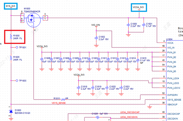
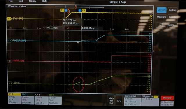
Would you help share your comments on OVPGDRV (tps65941212) behaviors when the Vsys_sense and VCCA reach 3.3V but Enable pin keep low during power up ?

Are the vsys monitor and OVPGDRV output controlled by Enable pin?

Thanks 

  • Hi Ted,

    Please see section: "8.3.1 System Supply Voltage Monitor and Over-Voltage Protection" for details on the OVPGDRV functionality.

    the OVPGDRV reaction is based on Vsys_sense. Enable does not affect OVPGDRV functionality.

    Thanks,

    Daniel W

  • Hi Daniel

    Thanks for your comments.

    What parts inside Leo will be controlled by Enable pin?

  • Hi Daniel

    Customer used tps65941212/1111 to provide the power supply to TDA4VM PDN-0B reference design. 

    you can find the part of LeoA schematic for refernce.

    Below scope waveforms between Vsys_sense, OVPGDRV, Enable and VCCA.  Would you help share your comments how to remove the red marked pulse with cycle at OVPGDRV output waveform during start-up?  After the system powered up, the system worked normally and no unexpected intterrupts were found in regisister 0x5A-0x6C. 

    Thanks 

  • Hi Ted,

    This appears to be the FET short test described in the below excerpt from the datasheet.

    "The diagnostic mechanism pulls the OVPDGRV pin low when VCCA reaches VOVP_FET_Short_TH, and waits until the voltage on the VCCA pin decreases by VOVP_FET_Short_Hyst before it pulls the OVPGDRV pin high again"

    Thanks,

    Daniel W