Hi Team,
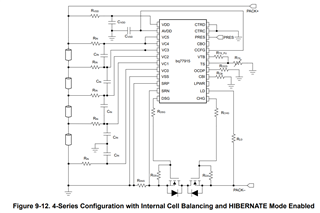
Our customer would like to ask your help to review the schematic diagram of his BQ77915 battery balancer design. His application is 4S li-ion battery pack and here is the schematic diagram.
Regards,
Danilo
This thread has been locked.
If you have a related question, please click the "Ask a related question" button in the top right corner. The newly created question will be automatically linked to this question.
Hi Team,
Our customer would like to ask your help to review the schematic diagram of his BQ77915 battery balancer design. His application is 4S li-ion battery pack and here is the schematic diagram.
Regards,
Danilo
Hi Danilo,
The schematic looks good for the most part, but there are a couple things I noticed:

Best,
Andria