This thread has been locked.

If you have a related question, please click the "Ask a related question" button in the top right corner. The newly created question will be automatically linked to this question.

Buck converter VFF control mode

Hi Team,

I'm studying about VM & VFF control mode currently. I have some questions as below:

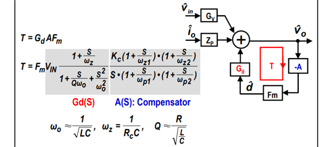
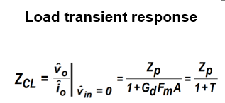
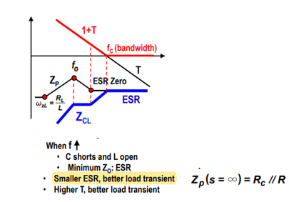
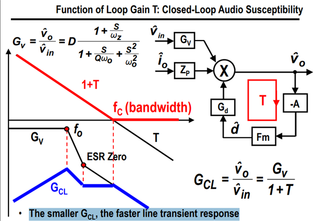
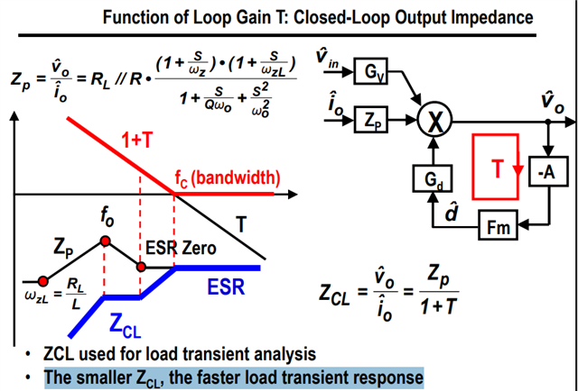
1. Line transient response & Load transient response. Could u please kindly explain why the smaller GCL and smaller ZCL could cause faster load transient response? What factors influence line/load transient response? Could u please offer related documents if there are?

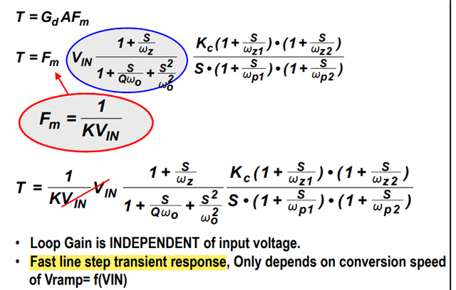
2. About VFF control mode, the ramp slope varies with Vin. How to understand this causes a faster line transient response than VM control mode? And how to get this equation Fm=1/(K*Vin), that's to say why (D/Vcomp)=1/(K*Vin)? Can we still prove it by similar trangles?


3. How to get this red 1+T bode plot in the question 1?I'm kinda confused. Could u please kindly explain how to get 1+T bode plot from T(Buck converter VM control mode control loop gain) bode plot?

Thanks a lot! Have a nice holiday!

Victoria

  • Hello Victoria,

    Thank you for reaching out.

    If you observe from the equations of GCL and ZCL, smaller GCL and ZCL means larger loop gain(T). It means that the larger loop gain increases the bandwidth (crossover frequency increases) as shown in the below figure. Higher the crossover frequency, faster the transient response but there is a limit for the crossover frequency based upon your switching frequency of the converter. Please have a look in Experiment 3 in this document (PMLK Buck Experiment Book (Rev. B) (ti.com)) to observe how the crossover frequency influence the transient response. 

    1+T is the desired loop gain of the converter. So based upon the compensation network you designed it changes.

    I would recommend the following documents to understand more about feedback loop and stability

    Practical-Feedback-Loop-Design-Buck.pdfslup340.pdf4276.slup206.pdf

    Thank you,

    Regards,

    Moheddin.

  • Hi Moheddin,

    Thanks for your wealth of documents, especially the slup340 which helps a lot! 

    About the question1, I mistook the close loop transfer function with the open loop transfer. Now I think I understand what u explained. Thanks for that! 

    I have a new question, ,from the equations of GCL and ZCL, can we think that a higher T offers a better perturbation suppression of vin to vo and io to vo? And in the process of loop design, what can we do practically to get higher T to make response faster?  

    About the question 2 , could u please kindly help to explain it? How is the Fm related with the pwm ramp slope? Can we still get Fm by similar trangles method?

    Thanks a lot! 

    Victoria 

  •  Hello Victoria,

    I will get back to you tomorrow with more information.

    Thank you,

    Regards,

    Moheddin.

  • Hello Victoria,

    I have a new question, ,from the equations of GCL and ZCL, can we think that a higher T offers a better perturbation suppression of vin to vo and io to vo? And in the process of loop design, what can we do practically to get higher T to make response faster?  

    It depends upon the compensation network you designed for your converter. There are some limitations as well for higher T (Higher crossover frequency). generally, you choose crossover frequency as 20% of your converter switching frequency.  You can find more about it in the document i shared (4276.slup206.pdf).  Please refer section F. Feedback loop design to understand more about the limitations. 

    About the question 2 , could u please kindly help to explain it? How is the Fm related with the pwm ramp slope? Can we still get Fm by similar trangles method?

    I will get back to you soon.

    Thank you,

    Regards,

    Moheddin.

  • Hi Moheddin,

    Thanks for your reply!  Sure, take your time.

    I have a new question now. About Buck converter VM control mode, the physical meaning of ZCL(close loop output impdedance) is load transient response. In the picture as below, Zp is open loop output impedance. T is VM mode loop gain. Here says in picture: Smaller ESR(the value is Rc//R) causes better load transient. Could u please explain the reason from this bode plot ? It seems not related with loop gain T.

    Best regards,

    Victoria

  • Hello Victoria,

    For example, consider two buck converters with different output capacitors having different ESR values. If you design the same compensation network for the two converters the crossover frequency varies since the open loop gain F(zero) changes due to change in ESR. which further effects the transient response.

    Now let us consider in different scenario, consider that the two buck converters having same crossover frequency even though they have different ESR. Since the compensation is made in such a way that both the converters achieve same crossover frequency. Irrespective of T (crossover frequency) the transient response varies due to ESR as shown in the equation below.

    Since the output filter inductor current iL cannot follow the fast-changing load current io, some extra current ic, goes through the output capacitor C and its equivalent series resistance (ESR). Both the capacitor C charge and the ESRc voltage drop form the output voltage spike that occurs in the transient.

    Therefore, we use the parallel output capacitors to reduce the ESR.

    Thank you,

    Regards,

    Moheddin.

  • Hey Moheddin,

    Really thanks a lot for explanation from 2 views: time domain and frequency domain. You made it much clear by time domain analysis. Could u please explain more about this? How does ESR value influence open loop gain?

    the open loop gain F(zero) changes due to change in ESR

    Thanks&best regards,

    Victoria

  • Hello Victoria,

    As the ESR value increases the frequency of ZERO decreases. which shown in the below picture.

    Thank you,

    Regards,

    Moheddin.