Other Parts Discussed in Thread: LM25145
Hi Team,
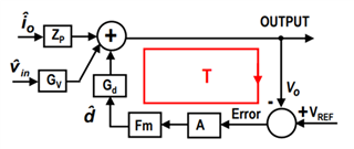
I',m studying about VFF control mode recently. There is a document shows the pwm modulator gain which is the second picture. We can see from it the VIN is the den of Fm so that it can be canceled by VIN in Gd transfer function part. It makes sense and easy to understand.

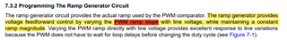
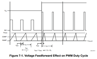
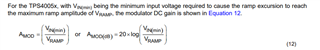
But in TPS40057 datasheet , I'm kinda confused about this, as seen in picture below. Why here says the VIN is the num of the modulator DC gain which conflicts to the upper document. And meanwhile I can't understand this sentence well 'with VIN(min) being the minimum input voltage required to cause the ramp excursion to reach the maximum ramp amplitude of VRAMP'. Could u please kindly help to clarify it?
Thanks a lot! Have a nice holiday!
Victoria