This thread has been locked.

If you have a related question, please click the "Ask a related question" button in the top right corner. The newly created question will be automatically linked to this question.

TLV733P: X2SON footprint solder mask defined: supplier ask to set solder mask = pad size

Part Number: TLV733P


Hello,

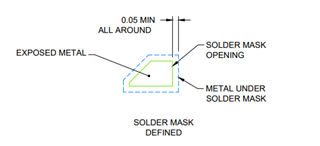
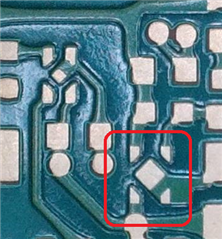
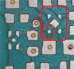
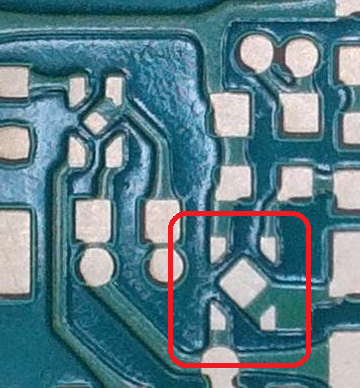
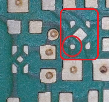
my supplier asked me to increase the solder mask opening to the size of the pad size.

https://www.ti.com/lit/ml/qfnd355c/qfnd355c.pdf

I created the footprint following our drawing of the DQN0004A.

Now the supplier has difficulties to create the small opening in the solder mask for pin 1 to 4. He is asking me to increase the solder mask to the pad size.

Does this greater opening of the solder mask influence solderability or there other mechanical concerns from your side?

Electrically it shouldn't have any influence.

Best regards,

David

  • Hi David, 

    Are you referring to the board layout or the Stencil Design?

    Technically, the following should work: 

    The main concern of perhaps increasing the solder mask to the pad size is the risk of creating a short when going through the reflow process. 

    Best, 

    Edgar Acosta

  • Hi Edgar,

    I refer to the board layout.
    As you show in the picture, the Solder Mask Opening is the topic in question.

    My supplier states it is to small and I should increase it to the size of Metal Under Solder Mask.

    I share the same concern of potential risk of a short. But the amount of solder paste is not increased.
    My hope is, that you have some data from the X2SON footprint development regarding variations and tolerances of the solder mask application process from different suppliers and you would say: "It's not ideal like shown in the datasheet but is not know to be an issue so far."

    Or the other way round... the following pictures show what I got from my supplier. He states the PCB is within tolerances and the Pad in the right picture is fine from his tolerances point of view. Do you know that this can happen to X2SON footprints? Is this smaller opening still within the tolerances for the X2SON package to be solderd correctly?

    After writing all above, I guess my real question is: Can I keep the footprint as shown in the datasheet and the solder mask opening is acceptable or should I increase the solder mask opening and make sure my supplier can work with that.

    Or in the end I have to figure it out myself?

    Thanks in advance for any information.

    Best regards,
    David

  • Hi David, 

    This picture seems correct to me: 

    What we show in the DS are only examples and guidance and that is what we use when we design our EVMs as well. 

    It will also depend on each supplier and their capabilities, but we know that there will be some tolerances that will be slightly different from what is shown in the DS, however I have not experienced any issues. 

    I would be more worried about the following image: 

    Where it might not be enough to properly solder the device. 

    I can run this by the packaging group to see if they have any thoughts/concerns regarding this. 

    Best, 

    Edgar Acosta

  • Hi Edgar,

    It would be very great, if you could run this by the packaging group.
    Thanks in advance.

    Best regards,

    David

  • Hi David, 

    I apologize for the delayed response. 

    I am still waiting a response from the packaging group. I followed up yesterday. 

    Best, 

    Edgar Acosta