


Hi team,
My customer is designing the PCB layout of this device.
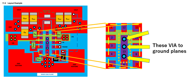
They are reffering to the layout example shown in the datasheet and have one question about it.
It seems that the 3 VIAs under the thermal pads (please see the attached figure) are for heat dissipation.
Can they remove this VIAs?
Are this VIAs nessesary from the heat dissipation point of view?
Regards,
Ohashi

