This thread has been locked.

If you have a related question, please click the "Ask a related question" button in the top right corner. The newly created question will be automatically linked to this question.

UCC2897A: PMP20742 based design with problems

Part Number: UCC2897A
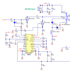
Other Parts Discussed in Thread: PMP20742

Hello,

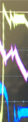
we have a design based on PMP20742 which shows a problem with the output voltage. The voltage drops, it looks like the UCC2897A goes into standby/disabled mode when this happens. The reference voltage Vref drops to zero in this case (this is seen approx. once in a second), but sometimes it also stays high.

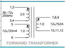
I attached a photo from the scope, yellow is Vout, blue is Vfb, purple is Vbias

As Vbias drops belov 8V I assume, that this could be the reason for the controller to go in a disabled mode or restart. I already tried to increase the bias capacitor without success. 

  • Hi T.K.

    You are correct, the bias voltage decaying to 8V is the reason the controller is being (momentarily) disabled.  The bias voltage should not be decaying when Vout is at the setpoint (12V).

    The reference design used 100 uF for the bias capacitor.  What values did you try?

    What other changes did you make to the reference design schematic (transformer, switching frequency, MOSFETs, opto-coupler, compensation, etc)?  I would use the reference design as a guide and double-check all components and values.

    Regards,

    Eric

  • I did not change any of the parts except not using the exact same ceramic caps. I tried 470 µF as C15, because I had one lying around.

    Is there a way to find out why the Vbias drops so low?

  • HI T.K.

    Can you please provide a PDF schematic?  Exactly which ceramic capacitors did you change?

    I would disconnect VBIAS from the AUX winding of the transformer and drive VBIAS with an external supply.  Make sure you set the current limit of the supply to something "low", like 100mA-200mA.  Then examine how the circuit operates.

    Initial startup of the PMP20742 looks like the following.  How does the initial startup of your design look?

    Did you use the exact same transformer from Pulse (PA2398NL) and output inductor (PDO120.113NL)?

    Is the opto-coupler and it's connections/bias the same?

    What is your input voltage?

    Good luck,

    Eric

  • The schematic is basically the same as the PMP20742 with some output regulators added for multiple voltages. The parts are the same except for the MLCC where some of the parts were not available. They are replaced by caps with same capacitances.

    Here you can see the startup of the design. Vout in yellow, Vbias in blue.

    I disconnected the AUX winding and supplied the 12.8 V to bias directly and the circuit started delivering 12 V. The current drawn at 12.8 V was 35 mA.

  • Hi T.K.

    The AUX winding cannot supply enough current to keep BIAS from decaying.  There is unusually high current flowing from the AUX and/or BIAS nodes.  Are any of the "additional" output regulators connected to BIAS or AUX?

    The UCC2897A controller itself should draw less than 3 mA (see below).  VDD current above 3 mA flows to the MAIN MOSFET and the AUX MOSFET.  Based on your measurement of 35 mA total, your FETs are drawing 32 mA (35 mA - 3 mA).  This seems like a lot.

    Can you verify the gate drive network on your AUX MOSFET, see below (C11, D5, and R3).

    Also, what did you use for MOSFETs, D6, D8, and L2?

    Regards,

    Eric

  • I checked the parts used in the gate drive network, with C11 being 100 nF, D5 BAS316 and R3 10k.

    The main FET is IRF7815PBF, the AUX FET is SQJ431AEP due to supply issues. D6, D8 are BAS316, L2 is a LPS4414-105M.

    I measured the gate drive signals of the FETs which are -11.6 V for the AUX FET and 12.8 V for the Main FET measured against GND. Aux switches first, then the main switches, turning off in opposite order. The duty cycle of this driving PWM is 33.6%.

    I further calculated the current draw from the decay rate of the bias voltage and the capacitance which leads to approx. 20 mA. Increasing the capacitor C15 (tried 900µF) only decreases the restart frequency, but never establishes a running design.

  • I disconnected the FETs from the PCB and measured the current through Vdd which is 3.5 mA when Vin is at 0 V and 6.1 mA when Vin is at 54V.

  • OK.  We know the regulator works with an external power supply in place of AUX/BIAS and draws 35 mA.  The Pulse transformer (PA2398NL) was designed for only 20 mA from the AUX winding, see PA2398NL diagram below.  I think we need to reduce the current from the AUX winding.

    The gate drive current is proportional to switching frequency and gate charge of the two MOSFETs.

    1) Check the switching frequency.  It must be 250 kHz, or slightly less.

    2) Your MAIN MOSFET is unchanged from the reference design, IRF7815.  However, the AUX MOSFET was changed from IRF6216 (150V/2.2A/0.24ohms) to SQJ431 (200V/9.4A/0.3ohms).  The SQJ431 is a much larger device and the gate charge and drive current are higher:  33nC_typ, 49nC_max, versus 55nC_typ, 85nC_max.

    IRF6216

    SQJ431

    After you check the switching frequency is <= 250 kHz, can you find a different AUX MOSFET that has gate charge more in-line with the IRF6216?  This should reduce the AUX current.

    What is your Vin during switching?

    Eric

  • The switching frequency is 249.37 kHz. I had a Si4455DY at hand which I soldered in. No big improvement, still the same characteristics.

    The current draw from Vdd is now 21.3 mA when externally supplied with 12.8 V.

    I always use 54 V as Vin as this supply is used in a PoE application.

  • Hi T.K.

    Please send your schematic for review.

    Also, can you take some 'scope pictures when Vout is regulating at 12V?  Look at Vout, VBIAS (after the diode), VAUX (before the diode), OUT pin, VREF, etc.  Use a short time-base, so we can see 5-10 switching cycles.

    Thanks,

    Eric