This thread has been locked.

If you have a related question, please click the "Ask a related question" button in the top right corner. The newly created question will be automatically linked to this question.

TPS7A57: REF_PIN CTRL MECHANISM

Part Number: TPS7A57

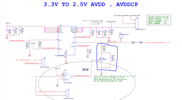
We have used this LDO in our design and below is sch for for circuit implementation.

Initially this regulator o/p should be set it to 1.1V and then after 20mS it should set it to 2.5V.

To implement this, we have used the MOSFET circuit as per the below image.

Please check and provide the feedback. Also please provide us the suggestion.

  • Hi Dhanabal,

    The device was not characterized under these conditions, however I do not see anything wrong with modifying the Rref resistance to force the device to behave differently. The change in VOUT will be dependent upon C771 as that capacitor will also need to charge up to the new 2.5V before the reference can operate in the unity gain configuration at that voltage.

    Regards,

    John

  • Can you please help to explore more on this?

  • The change in VOUT will be dependent upon C771 as that capacitor will also need to charge up to the new 2.5V before the reference can operate in the unity gain configuration at that voltage. - How to achieve this? 

  • Hi Dhanabal, 

    Once the LDO is operating, there is an internal switch that closes between REF and NR/SS. Therefore, there will be an RC delay when you implement the voltage margin. This RC delay will depend on the Resistor at REF and the capacitor at NR/SS, hence the reference to C771. This is also shown in the TPS7A57 DS. It will take ~235ms to change from 1.1V to 2.5V and not 20ms.

    Notice from the DS, when using a DAC with current output mode and targeting a +- 2.5% margin with 1.8V nominal, it takes ~169ms to change from 1.8V to 1.8045 since Cnrss=4.7uF and Rref=36kOhms:

    In addition to this, a change from 1.1V to 2.5V is still doable with a single DAC if using an Output-Current capable DAC, and/or using a DAC plus an extra resistor if using the Voltage Output mode. This can help minimize the number of components and complexity of the design.

    Best, 

    Edgar Acosta