This thread has been locked.

If you have a related question, please click the "Ask a related question" button in the top right corner. The newly created question will be automatically linked to this question.

TPS546D24A: transient spec failed

Part Number: TPS546D24A


Hi team,

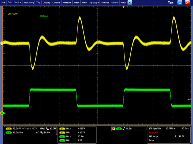
they try 3.3V with 0.68uH , 650kHz and code 28 today , transient all failed, 

would you advised which should they change to improve?

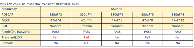
for example , the tolerance is +-5%, the maximum 3.465V barely have any margin.

Copy of TPS546D24A_CPUB 3.3V setting_20221201.xlsx

  •  

    The Provided Oscilloscope waveform shows passing a 3.3V +/- 5% ( 3.135 - 3.465) specification, including both ripple and transient, and that is under a load transient 2 1/2 times higher than the 6.6A transient that was provided in the XLS design document.

    If you can advise what the actual specification is, in terms of transient current amplitude, and allowable output voltage deflection, I can help provide a recommendation.

    You can try Compensation Code 29, but this places the cross-over right at the POSCAP ESR-zero / Inductor MLCC-resonance cross-over where the slope of the loop gain is flat making the loop's stability and bandwidth susceptible to large variations due to layout parasitics and component variations.

  • Hi Peter,

    sorry for forgetting the detail, the waveform we've shown is the best one out of  five transient test (9xPOSCAP + 12 MLCC),

    and you're right, they want Vout within 3.3V +/- 5% ( 3.135 - 3.465), even 3.465V is still a fail to them because they need more margin. 

    and about the 6.6A in the excel was wrong, because we don't know what " load release transient current" means, 

    we only know transient step is (100%-30%)x20=14A

    can you guide us on what should we input ?

    and so you're suggestion for better transient  now is to change code from 30 to 29, right?

  •  

    The "Load Step / Load Release Transient Current" is the amplitude of the Load Step (Increase) or Load Release (Decrease) in the loading current.

    If the load step / load release is 30% - 100% and 100% to 30% then it would be 70% of the full load current, or 14A

    Based on meeting a <165mV overshoot and undershoot on a 14A dynamic load change  (11.7mΩ output impedance) I would recommend pin programmable Compensation Code 29 rather than Compensation Code 28.  Compensation Code 28 provided enough voltage loop gain to meet the 165mV over/under shoot with a 6.6A transient but is not sufficient to meet that with a 14A transient.  Compensation Code 29 should be able to meet the 165mV transient, though the margin is relatively small.

    If they need additional margin, they may need to use COMPENSATION CODE 30, but the VLOOP GAIN = 8.

    I see that Compensation Code 8 is stable with 3x 330μF 9mΩ POSCAPs plus 4x 47μF MLCCs though the phase is dropping rapidly at crossover, so the gain margin is low and the design would benefit from some additional MCLL capacitors.

  • Hi Peter,

    thanks they pass with code 30, 

    but you mentioned  "but the VLOOP GAIN = 8"    when you recommended code 30 yesterday.

    what does this mean ? is there something wrong I should concern when VLOOP GAIN=8?

    and is there a reason  why we have to keep the ILOOP/VLOOP ratio in green in the excel?

  • but you mentioned  "but the VLOOP GAIN = 8"    when you recommended code 30 yesterday.

    Sorry, it looks like there was an errant return, and the next line finishes the thought.

    but the VLOOP gain = 8.  I see that Compensation code 30 (VLOOP = 8) is stable with 3x 330μF 9mΩ POSCAPS plus 4x 47μF MLCCs, through the phase is dropping rapidly at crossover, so the gain margin is low and the design would benefit from some additional MLC Capacitors.

    My apologies about that confusion.

    and is there a reason  why we have to keep the ILOOP/VLOOP ratio in green in the excel?

    When the ILOOP / VLOOP bandwidth ratio is less than 2, the phase margin in the voltage loop tends to be low, so we warn the user about this.  If they are comfortable with the low voltage-loop phase margin and its performance, an ILOOP / VLOOP ratio under 2 can be tolerated.

    In multiphase applications, an ILOOP / VLOOP ratio less than 2 will also reduce the dynamic current sharing between the phases somewhat.

  • Hi Miller,

    thanks code 30 has passed the spec.

    BTW,

    by " the phase margin in the voltage loop " you mean the independent PM only in the voltage loop?

    as long as the total Phase margin is good, we shouldn't care about the independent PM of voltage loop and current loop, right?

  •  

    The voltage loop does not have an "independent phase margin"  When you measure the outer feedback loop bode plot, you are measure the gain and phase of the voltage regulation loop.

    If the measured gain and phase of the outer voltage regulation loop are acceptable, then the 2:1 ILOOP : VLOOP bandwidth guidance can be effectively dismissed.

    It is the gain and phase of the inner current loop that can not be easily measured due to the difficulty in measuring switching current and the fully internal feedback of the current loop, making injecting an sine-wave into the feedback and measuring the resulting current regulation result difficult.

  • Hi Peter,

    sorry , what's the definition of the inner current loop?

    I thought is the blue one ( GMI )

    please correct me if I'm wrong.

  •  

    The Inner Current Loop includes the GMI transconductance amplifier, it's RVI, CZI and CPI compensation, the TON generator, MOSFET drivers, MOSFETS, Inductor, which controls the TO to Switch Current transfer function,  the switch current sense on the high-side and low-side MOSFET and their current sense gain amplifier that then drives the I_SNS input to the GMI current error amplifier.

    The purpose of the inner current loop is to match the averaged sensed switch current (I_SNS) to its control signal VSHARE, which sets the "reference" for the current control loop.

  • Hi Peter,

    but if we measure the outer feedback loop bode plot, I though the path include VLOOP (green) and ILOOP (blue) ,

    but you said we only can measure  VLOOP actually, may I know why?

  •  

    When you break the feedback path, inject and monitor the feedback, you will be able to observe the Bandwidth, Gain and Phase margin of the outer voltage loop, as it is influenced by the inner current loop, but you will not be able to measure the bandwidth, gain, or phase of the inner current loop, only its influence on the outer voltage loop.

    While you can see the effect that changing the inner current loop's bandwidth on the outer voltage loop with the change in high-frequency phase margin, you are not actually monitoring the current loop, just its indirect influence on the outer voltage loop.

  • Hi Peter,

    on the other hand,

    you said 2:1 ratio ,

    by Vloop in this 2:1 ratio, you mean this internal part below or you mean the whole outer voltage loop of converter?

  •  

    The bandwidth of the overall voltage loop from V0SNS, through the internal VOUT_SCALE_LOOP divider, voltage error amplifier, current error amplifier, Pulse Width Modulator, Drivers, MOSFETs, inductor, Output and back to VOSNS should be 1/2 the bandwidth of the inner current loop from switch current sense (I_SNS) through the current error amplifier, to the PWM generator, to the drivers, to the FETs, and the current sense amplifier back to the I_SNS.

    That ensures that the VSHARE signal, which is the reference for the inner current loop, is relatively constant within the bandwidth of the inner current loop.