This thread has been locked.

If you have a related question, please click the "Ask a related question" button in the top right corner. The newly created question will be automatically linked to this question.

TPS63020 PS/SYNC and VINA Connections

Other Parts Discussed in Thread: BQ24020, TPS63020

Hi,

Q1: Can the PS/SYNC pin (power safe mode) be active for good?


Q2: Should the VINA pin be also connected to VIN or is it internal connected?


Q3: from page 12 from the PDF file it seems that there are six capacitors, from the layout point of view (page17) there are additional two more capacitors.

Please send me TI recommended application notes for Vout-5V


Please find Q4 regarding the GND and power ground of the TP63020 and bq24020.

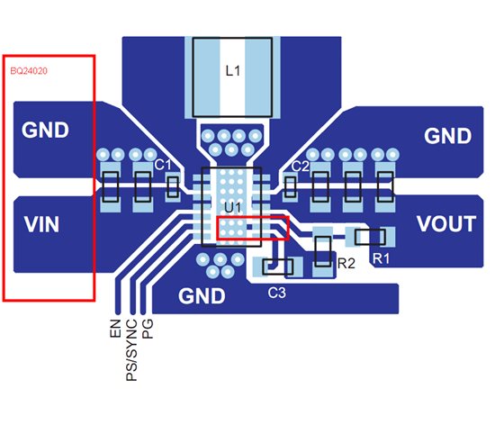
Q4: the charger bq24020 powers up (VIN) the SPS TP63020. Can the charger ground be the same plan as the SPS GND pin 2. In all hoe should the ground separation between the two IC be like. A sketch will be fine.

Thanks,

Shlomi

  • Generally, we recommend you follow the design procedure in the datasheet and your schematic and layout match that of the EVM. 

    See my comments below:

    Shlomi Yehezkia said:

    Q1: Can the PS/SYNC pin (power safe mode) be active for good?

    [D.A.] PS/SYNC is an input to enable power save mode or for a system clock. Per the description on page 13 of the datasheet, grounding this pin allows the converter to enter power save mode at light loads; pulling this pin high forces the device to remain in PWM mode for all loads. Or instead, a system clock can be applied between 2.2MHz and 2.6MHz to synchronize multiple power supplies. 
    Did you mean output PG (power good) pin? PG, open-drain output, should have a 1 M Ohm pull-up to Vout and is '1' when power is good and '0' otherwise. 
    Q2: Should the VINA pin be also connected to VIN or is it internal connected?
    [D.A.] VINA should be connected to a 0.1uF ceramic capacitor. VINA has an internal connection to VIN and does not need to be externally connected to VIN. 
    Q3: from page 12 from the PDF file it seems that there are six capacitors, from the layout point of view (page17) there are additional two more capacitors.
    [D.A.] The additional pads on the layout are un-populated and are available to add more input/output filtering capacitors.  
    Please send me TI recommended application notes for Vout-5V
    [D.A.] To design for Vout = 5 V, you will need to also specify Vin and at least your output current. You can follow the design procedure in the datasheet and use Switcher-Pro free design software to aid in the design. 
    Please find Q4 regarding the GND and power ground of the TP63020 and bq24020.
    Q4: the charger bq24020 powers up (VIN) the SPS TP63020. Can the charger ground be the same plan as the SPS GND pin 2. In all hoe should the ground separation between the two IC be like. A sketch will be fine.
    [D.A.]  No. The BQ24020 charger needs to be connected to power ground of the TPS63020. The TPS63020 Pin 2 GND should be connected TO PGND only under the IC.


  • See my comment in red

    Generally, we recommend you follow the design procedure in the datasheet and your schematic and layout match that of the EVM

    See my comments below:

    Q1: Can the PS/SYNC pin (power safe mode) be active for good?

    [D.A.] PS/SYNC is an input to enable power save mode or for a system clock. Per the description on page 13 of the datasheet, grounding this pin allows the converter to enter power save mode at light loads; pulling this pin high forces the device to remain in PWM mode for all loads. Or instead, a system clock can be applied between 2.2MHz and 2.6MHz to synchronize multiple power supplies. 

    Did you mean output PG (power good) pin? PG, open-drain output, should have a 1 M Ohm pull-up to Vout and is '1' when power is good and '0' otherwise. 


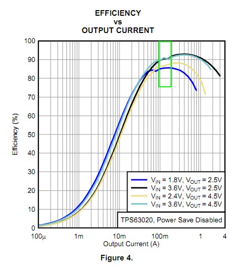
    During my operation my system can encounter low loads (100-200mA) and high loads (1A- during transmissions), so in order to exceed high efficiency at  low and high loads, can the PS pin remain low for such application.?


  • If you connect PS/SYNC low, the TPS63020 will automatically transition between power save mode and PWM mode as the load varies. 

    In your case, where the load is always greater than 100 mA, the TPS63020 will not enter power save mode; however, at 100-200 mA loads the efficiency of PWM mode is still relatively high (greater than 80% if you follow the design and layout of the EVM).