Hi,
Q1: Can the PS/SYNC pin (power safe mode) be active for good?
Q2: Should the VINA pin be also connected to VIN or is it internal connected?
Q3: from page 12 from the PDF file it seems that there are six capacitors, from the layout point of view (page17) there are additional two more capacitors.
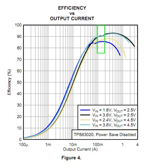
Please send me TI recommended application notes for Vout-5V
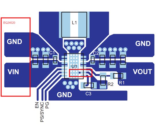
Please find Q4 regarding the GND and power ground of the TP63020 and bq24020.
Q4: the charger bq24020 powers up (VIN) the SPS TP63020. Can the charger ground be the same plan as the SPS GND pin 2. In all hoe should the ground separation between the two IC be like. A sketch will be fine.
Thanks,
Shlomi