This thread has been locked.
If you have a related question, please click the "Ask a related question" button in the top right corner. The newly created question will be automatically linked to this question.
Can a shielded inductor be placed directly below the IC like in the picture?
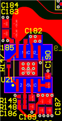
We have limited space and we are not sure would this radiate too much. The PCB thickness is standard 1.6mm and the number of layers is yet unknown, but will be at least 10, so there are multiple GND planes.
Thanks
Filipa
Hi Filipa,
Miranda will review it and reply you later this week due to sick leave.
Hi Filipa,
Usually we recommend that the inductor and output capacitors are on the same layer with IC, otherwise the vias from top layer to bottom layer would increase parasitic and the power loop is too long which cause jitter and EMI issue.
If we must use this layout and our application is not sensitive to the jitter, you can try this and have some tests about the output voltage ripple.
Actually this again wasn't the answer on my question. My question is a radiation from the shielded inductor itself (placed directly below the IC). Not the power loop
Hi Filipa,
Regarding the radiation from the shielded inductor itself, it's ok for the device.