This thread has been locked.

If you have a related question, please click the "Ask a related question" button in the top right corner. The newly created question will be automatically linked to this question.

BQ76952: Thermistor value shows inaccurate in BQ76952

Part Number: BQ76952

Hello sir.

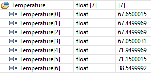
We are using BQ76952 for battery management with STM32 using I2C protocol,but unfortunately we can't get the actual temperature of Thermistor. We use 18k thermistor (10k in room temperature). We connect 6 thermistors on TS1, TS3, HDQ, CFETOFF, DDSG & DCHG pin. But we get inaccurate values. After Temperature offsets (TS1TempOffset, CFETOFFTempOffset, TS3TempOffset, HDQTempOffset, DCHGTempOffset, DDSGTempOffset) we are getting values average 70 degree C on each thermistor. But the real temperature should be near 30 degree C.

Internal temperature shows correct (IntTemperature 0x68). 

Please help to solve this problem. Looking for positive reply.

Regards,

Subhrajit Majumder.

  • Hi Subhrajit,

    Have you used the BQ769x2 thermistor coefficient calculator to update the coefficients for the thermistor you selected? The tool and instructions are located here: https://www.ti.com/tool/BQ769X2-THERMISTOR-COEFF-CALCULATOR

    Best regards,

    Matt

  • Dear Matt,

    In the thermistors.txt file how to find the registance value, can I use multimeter to measure the registance. In my case the registance value is 10k ohm.

    And how can I find the  Temperatures (degreesC)?  May I need to specified the Thermistor temperature range?

  • The thermistor datasheet should have a table of thermistor resistance vs. temperature. You need to find this table for your thermistor.

  • Thankyou very much for your help Matt.
    Will update soon regarding the result.

    Regards,

    Subhrajit Majumder.

  • Dear Matt, 

    After getting the coefficient I need to put the value at TS1TempOffset, CFETOFFTempOffset, TS3TempOffset, HDQTempOffset, DCHGTempOffset, DDSGTempOffset for the better result?

  • The coefficients go into the Calibration:18K Temperature Model registers. This should be explained in the instructions and the device TRM.

  • Dear Matt,

    There are total 10 Calibration:18K Temperature Model like Calibration:18K Temperature Model:Coeff a / Calibration:18K Temperature Model:Coeff b  / Calibration:18K Temperature Model:Adc0.

    Particulately in which registor I need to set the coefficient? 

  • Have you received results from the tool? The report will tell you the parameters and values for each parameter you need to enter. 

  • Yes sir. 

    We received the value and we place it. But no difference shows. I attached the output as well.

    ********************************
    Search complete, bestmaxerr = 0.20000000000001705
    bestA [A1 A2 A3 A4 A5] = [-16669 31696 -27396 26324 1370]
    bestB [B1 B2 B3 B4] = [-2110 3962 -4296 4750]
    Adc0 = 11703
    ******************************

    These value we receive from  BQ769x2 thermistor coefficient calculator.

    I attached my code as well where I put the coefficient value.

    // 18k Temperature model
    BQ769x2_SetRegister(T18kCoeffa1, 0xBEE3, 2); // 18k Temp a1
    BQ769x2_SetRegister(T18kCoeffa2, 0x7BD0, 2); // 18k Temp a2
    BQ769x2_SetRegister(T18kCoeffa3, 0x94FC, 2); // 18k Temp a2
    BQ769x2_SetRegister(T18kCoeffa4, 0x66D4, 2); // 18k Temp a4
    BQ769x2_SetRegister(T18kCoeffa5, 0x055A, 2); // 18k Temp a5
    BQ769x2_SetRegister(T18kCoeffb1, 0xF7C2, 2); // 18k Temp b1
    BQ769x2_SetRegister(T18kCoeffb2, 0x0F7A, 2); // 18k Temp b2
    BQ769x2_SetRegister(T18kCoeffb3, 0xEF38, 2); // 18k Temp b3
    BQ769x2_SetRegister(T18kCoeffb4, 0x128E, 2); // 18k Temp b4
    BQ769x2_SetRegister(T18kAdc0, 0x2DB7, 2); // 18k ADC 0

  • I attach my code as well..

    #include "main.h"
    #include "BQ769x2Header.h"
    /* Private includes ----------------------------------------------------------*/
    /* USER CODE BEGIN Includes */
    #define DEV_ADDR  0x10  // BQ769x2 address is 0x10 including R/W bit or 0x8 as 7-bit address
    #define CRC_Mode 1  // 0 for disabled, 1 for enabled
    #define MAX_BUFFER_SIZE 10
    #define R 0 // Read; Used in DirectCommands and Subcommands functions
    #define W 1 // Write; Used in DirectCommands and Subcommands functions
    #define W2 2 // Write data with two bytes; Used in Subcommands function
    uint8_t AFE_Flag= 1;
    HAL_StatusTypeDef res;
    /* USER CODE END Includes */
    
    /* Private typedef -----------------------------------------------------------*/
    /* USER CODE BEGIN PTD */
    
    /* USER CODE END PTD */
    
    /* Private define ------------------------------------------------------------*/
    /* USER CODE BEGIN PD */
    /* USER CODE END PD */
    
    /* Private macro -------------------------------------------------------------*/
    /* USER CODE BEGIN PM */
    
    /* USER CODE END PM */
    
    /* Private variables ---------------------------------------------------------*/
    I2C_HandleTypeDef hi2c2;
    
    TIM_HandleTypeDef htim16;
    
    /* USER CODE BEGIN PV */
    uint8_t RX_data [2] = {0x00, 0x00}; // used in several functions to store data read from BQ769x2
    uint8_t RX_2Byte [2] = {0x00, 0x00};
    uint8_t RX_3Byte [2] = {0x00, 0x00};
    uint8_t RX_4Byte [2] = {0x00, 0x00};
    uint8_t RX_5Byte [2] = {0x00, 0x00};
    uint32_t I_amp = 0x0000;
    uint8_t RX_32Byte [32] = {0x00, 0x00, 0x00, 0x00, 0x00, 0x00, 0x00, 0x00, 0x00, 0x00, 0x00, 0x00, 0x00, 0x00, 0x00, 0x00,
    	0x00, 0x00, 0x00, 0x00, 0x00, 0x00, 0x00, 0x00, 0x00, 0x00, 0x00, 0x00, 0x00, 0x00, 0x00, 0x00};
    	//used in Subcommands read function
    // Global Variables for cell voltages, temperatures, Stack voltage, PACK Pin voltage, LD Pin voltage, CC2 current
    uint16_t CellVoltage [16] = {0x00,0x00,0x00,0x00,0x00,0x00,0x00,0x00,0x00,0x00,0x00,0x00,0x00,0x00,0x00,0x00};
    float Temperature [7] = {0,0,0,0,0,0,0};
    uint16_t Stack_Voltage = 0x00;
    uint16_t Pack_Voltage = 0x00;
    uint16_t LD_Voltage = 0x00;
    int Pack_Current;
    int lc;
    uint16_t current = 0x00;
    
    uint16_t AlarmBits = 0x00;
    uint8_t value_SafetyAlertA;  // Safety Status Register A
    uint8_t value_SafetyAlertB;  // Safety Status Register B
    uint8_t value_SafetyAlertC;  // Safety Status Register C
    uint8_t value_SafetyStatusA;  // Safety Status Register A
    uint8_t value_SafetyStatusB;  // Safety Status Register B
    uint8_t value_SafetyStatusC;  // Safety Status Register C
    uint8_t value_PFStatusA;   // Permanent Fail Status Register A
    uint8_t value_PFStatusB;   // Permanent Fail Status Register B
    uint8_t value_PFStatusC;   // Permanent Fail Status Register C
    uint8_t FET_Status;  // FET Status register contents  - Shows states of FETs
    uint8_t value_FETOptions; //PreDischarge status
    uint16_t CB_ActiveCells;  // Cell Balancing Active Cells
    
    uint8_t	UV_Fault = 0;   // under-voltage fault state
    uint8_t	OV_Fault = 0;   // over-voltage fault state
    uint8_t	SCD_Fault = 0;  // short-circuit fault state
    uint8_t	OCD_Fault = 0;  // over-current fault state
    uint8_t	OCD_Fault1 = 0;
    uint8_t	OCC_Fault = 0;
    uint8_t ProtectionsTriggered = 0; // Set to 1 if any protection triggers
    
    uint8_t LD_ON = 0;	// Load Detect status bit
    uint8_t DSG = 0;   // discharge FET state
    uint8_t CHG = 0;   // charge FET state
    uint8_t PCHG = 0;  // pre-charge FET state
    uint8_t PDSG = 0;  // pre-discharge FET state
    uint8_t DCHG_pin = 0;
    uint8_t DDSG_pin = 0;
    uint8_t ALRT_pin = 0;
    uint8_t RSVD_pin = 0;
    
    uint8_t RSVD_00 = 0;
    uint8_t RSVD_01 = 0;
    uint8_t FET_INIT_OFF = 0;
    uint8_t PDSG_EN = 0;
    uint8_t FET_CTRL_EN = 0;
    uint8_t HOST_FET_EN = 0;
    uint8_t SLEEPCHG = 0;
    uint8_t SFET = 0;
    
    uint32_t CC1; // in BQ769x2_READPASSQ func
    uint32_t CC2;// in BQ769x2_READPASSQ func
    uint32_t CC3;// in BQ769x2_READPASSQ func
    uint32_t AccumulatedCharge_Int; // in BQ769x2_READPASSQ func
    uint32_t AccumulatedCharge_Frac;// in BQ769x2_READPASSQ func
    uint32_t AccumulatedCharge_Time;// in BQ769x2_READPASSQ func
    
    /* USER CODE END PV */
    
    /* Private function prototypes -----------------------------------------------*/
    void SystemClock_Config(void);
    static void MX_GPIO_Init(void);
    static void MX_I2C2_Init(void);
    static void MX_TIM16_Init(void);
    /* USER CODE BEGIN PFP */
    void delayUS(uint32_t us){
    	__HAL_TIM_SET_COUNTER(&htim16,0);  // set the counter value a 0
    		while (__HAL_TIM_GET_COUNTER(&htim16) < us);// wait for the counter to reach the us input in the parameter
    }
    
    void CopyArray(uint8_t *source, uint8_t *dest, uint8_t count)
    {
        uint8_t copyIndex = 0;
        for (copyIndex = 0; copyIndex < count; copyIndex++)
        {
            dest[copyIndex] = source[copyIndex];
        }
    }
    
    unsigned char Checksum(unsigned char *ptr, unsigned char len)
    // Calculates the checksum when writing to a RAM register. The checksum is the inverse of the sum of the bytes.
    {
    	unsigned char i;
    	unsigned char checksum = 0;
    
    	for(i=0; i<len; i++)
    		checksum += ptr[i];
    
    	checksum = 0xff & ~checksum;
    
    	return(checksum);
    }
    
    unsigned char CRC8(unsigned char *ptr, unsigned char len)
    //Calculates CRC8 for passed bytes. Used in i2c read and write functions
    {
    	unsigned char i;
    	unsigned char crc=0;
    	while(len--!=0)
    	{
    		for(i=0x80; i!=0; i/=2)
    		{
    			if((crc & 0x80) != 0)
    			{
    				crc *= 2;
    				crc ^= 0x107;
    			}
    			else
    				crc *= 2;
    
    			if((*ptr & i)!=0)
    				crc ^= 0x107;
    		}
    		ptr++;
    	}
    	return(crc);
    }
    
    void I2C_WriteReg(uint8_t reg_addr, uint8_t *reg_data, uint8_t count)
    {
    	uint8_t TX_Buffer [MAX_BUFFER_SIZE] = {0x00,0x00,0x00,0x00,0x00,0x00,0x00,0x00,0x00,0x00};
    #if CRC_Mode
    	{
    		uint8_t crc_count = 0;
    		crc_count = count * 2;
    		uint8_t crc1stByteBuffer [3] = {0x10, reg_addr, reg_data[0]};
    		unsigned int j;
    		unsigned int i;
    		uint8_t temp_crc_buffer [3];
    
    		TX_Buffer[0] = reg_data[0];
    		TX_Buffer[1] = CRC8(crc1stByteBuffer,3);
    
    
    		j = 2;
    		for(i=1; i<count; i++)
    		{
    			TX_Buffer[j] = reg_data[i];
    			j = j + 1;
    			temp_crc_buffer[0] = reg_data[i];
    			TX_Buffer[j] = CRC8(temp_crc_buffer,1);
    			j = j + 1;
    		}
    		HAL_I2C_Mem_Write(&hi2c2, DEV_ADDR, reg_addr, 1, TX_Buffer, crc_count, 1000);
    	}
    #else
    	HAL_I2C_Mem_Write(&hi2c2, 0x10<<1, reg_addr, 1, reg_data, count, 1000);
    #endif
    }
    unsigned int RX_CRC_Fail = 0;  // reset to 0. If in CRC Mode and CRC fails, this will be incremented.
    void I2C_ReadReg(uint8_t reg_addr, uint8_t *reg_data, uint8_t count)
    {
    //	unsigned int RX_CRC_Fail = 0;  // reset to 0. If in CRC Mode and CRC fails, this will be incremented.
    	uint8_t RX_Buffer [MAX_BUFFER_SIZE] = {0x00,0x00,0x00,0x00,0x00,0x00,0x00,0x00,0x00,0x00};
    #if CRC_Mode
    	{
    		uint8_t crc_count = 0;
    		uint8_t ReceiveBuffer [10] = {0x00,0x00,0x00,0x00,0x00,0x00,0x00,0x00,0x00,0x00};
    		crc_count = count * 2;
    		unsigned int j;
    		unsigned int i;
    		unsigned char CRCc = 0;
    		uint8_t temp_crc_buffer [3];
    
    		HAL_I2C_Mem_Read(&hi2c2, DEV_ADDR, reg_addr, 1, ReceiveBuffer, crc_count, 1000);
    		uint8_t crc1stByteBuffer [4] = {0x10, reg_addr, 0x11, ReceiveBuffer[0]};
    		CRCc = CRC8(crc1stByteBuffer,4);
    		if (CRCc != ReceiveBuffer[1])
    		{
    			RX_CRC_Fail += 1;
    		}
    		RX_Buffer[0] = ReceiveBuffer[0];
    
    		j = 2;
    		for (i=1; i<count; i++)
    		{
    			RX_Buffer[i] = ReceiveBuffer[j];
    			temp_crc_buffer[0] = ReceiveBuffer[j];
    			j = j + 1;
    			CRCc = CRC8(temp_crc_buffer,1);
    			if (CRCc != ReceiveBuffer[j])
    				RX_CRC_Fail += 1;
    			j = j + 1;
    		}
    		CopyArray(RX_Buffer, reg_data, crc_count);
    	}
    #else
    	HAL_I2C_Mem_Read(&hi2c2, 0x11, reg_addr, 2, reg_data, count, 1000);
    //	HAL_I2C_Master_Receive(&hi2c4, DEV_ADDR, reg_addr, 2, HAL_MAX_DELAY);
    #endif
    	return 0;
    }
    void BQ769x2_SetRegister(uint16_t reg_addr, uint32_t reg_data, uint8_t datalen)
    {
    	uint8_t TX_Buffer[2] = {0x00, 0x00};
    	uint8_t TX_RegData[6] = {0x00, 0x00, 0x00, 0x00, 0x00, 0x00};
    
    	//TX_RegData in little endian format
    	TX_RegData[0] = reg_addr & 0xff;
    	TX_RegData[1] = (reg_addr >> 8) & 0xff;
    	TX_RegData[2] = reg_data & 0xff; //1st byte of data
    
    	switch(datalen)
        {
    		case 1: //1 byte datalength
          		I2C_WriteReg(0x3E, TX_RegData, 3);
    			delayUS(2000);
    			TX_Buffer[0] = Checksum(TX_RegData, 3);
    			TX_Buffer[1] = 0x05; //combined length of register address and data
          		I2C_WriteReg(0x60, TX_Buffer, 2); // Write the checksum and length
    			delayUS(2000);
    			break;
    		case 2: //2 byte datalength
    			TX_RegData[3] = (reg_data >> 8) & 0xff;
    			I2C_WriteReg(0x3E, TX_RegData, 4);
    			delayUS(2000);
    			TX_Buffer[0] = Checksum(TX_RegData, 4);
    			TX_Buffer[1] = 0x06; //combined length of register address and data
          		I2C_WriteReg(0x60, TX_Buffer, 2); // Write the checksum and length
    			delayUS(2000);
    			break;
    		case 4: //4 byte datalength, Only used for CCGain and Capacity Gain
    			TX_RegData[3] = (reg_data >> 8) & 0xff;
    			TX_RegData[4] = (reg_data >> 16) & 0xff;
    			TX_RegData[5] = (reg_data >> 24) & 0xff;
    			I2C_WriteReg(0x3E, TX_RegData, 6);
    			delayUS(2000);
    			TX_Buffer[0] = Checksum(TX_RegData, 6);
    			TX_Buffer[1] = 0x08; //combined length of register address and data
          		I2C_WriteReg(0x60, TX_Buffer, 2); // Write the checksum and length
    			delayUS(2000);
    			break;
        }
    }
    void CommandSubcommands(uint16_t command) //For Command only Subcommands
    // See the TRM or the BQ76952 header file for a full list of Command-only subcommands
    {	//For DEEPSLEEP/SHUTDOWN subcommand you will need to call this function twice consecutively
    
    	uint8_t TX_Reg[2] = {0x00, 0x00};
    
    	//TX_Reg in little endian format
    	TX_Reg[0] = command & 0xff;
    	TX_Reg[1] = (command >> 8) & 0xff;
    
    	I2C_WriteReg(0x3E,TX_Reg,2);
    	delayUS(2000);
    }
    void Subcommands(uint16_t command, uint16_t data, uint8_t type)
    // See the TRM or the BQ76952 header file for a full list of Subcommands
    {
    	//security keys and Manu_data writes dont work with this function (reading these commands works)
    	//max readback size is 32 bytes i.e. DASTATUS, CUV/COV snapshot
    	uint8_t TX_Reg[4] = {0x00, 0x00, 0x00, 0x00};
    	uint8_t TX_Buffer[2] = {0x00, 0x00};
    
    	//TX_Reg in little endian format
    	TX_Reg[0] = command & 0xff;
    	TX_Reg[1] = (command >> 8) & 0xff;
    
    	if (type == R) {//read
    		I2C_WriteReg(0x3E,TX_Reg,2);
    		delayUS(2000);
    		I2C_ReadReg(0x40, RX_32Byte, 32); //RX_32Byte is a global variable
    	}
    	else if (type == W) {
    		//FET_Control, REG12_Control
    		TX_Reg[2] = data & 0xff;
    		I2C_WriteReg(0x3E,TX_Reg,3);
    		delayUS(1000);
    		TX_Buffer[0] = Checksum(TX_Reg, 3);
    		TX_Buffer[1] = 0x05; //combined length of registers address and data
    		I2C_WriteReg(0x60, TX_Buffer, 2);
    		delayUS(1000);
    	}
    	else if (type == W2){ //write data with 2 bytes
    		//CB_Active_Cells, CB_SET_LVL
    		TX_Reg[2] = data & 0xff;
    		TX_Reg[3] = (data >> 8) & 0xff;
    		I2C_WriteReg(0x3E,TX_Reg,4);
    		delayUS(1000);
    		TX_Buffer[0] = Checksum(TX_Reg, 4);
    		TX_Buffer[1] = 0x06; //combined length of registers address and data
    		I2C_WriteReg(0x60, TX_Buffer, 2);
    		delayUS(1000);
    	}
    }
    void DirectCommands(uint8_t command, uint16_t data, uint8_t type)
    // See the TRM or the BQ76952 header file for a full list of Direct Commands
    {	//type: R = read, W = write
    	uint8_t TX_data[2] = {0x00, 0x00};
    
    	//little endian format
    	TX_data[0] = data & 0xff;
    	TX_data[1] = (data >> 8) & 0xff;
    
    	if (type == R) {//Read
    		I2C_ReadReg(command, RX_data, 2); //RX_data is a global variable
    		delayUS(2000);
    	}
    	if (type == W) {//write
        //Control_status, alarm_status, alarm_enable all 2 bytes long
    		I2C_WriteReg(command,TX_data,2);
    		delayUS(2000);
    	}
    }
    
    void BQ769x2_Init() {
    	// Configures all parameters in device RAM
    
    	// Enter CONFIGUPDATE mode (Subcommand 0x0090) - It is required to be in CONFIG_UPDATE mode to program the device RAM settings
    	// See TRM for full description of CONFIG_UPDATE mode
    	CommandSubcommands(SET_CFGUPDATE);
    
    	// After entering CONFIG_UPDATE mode, RAM registers can be programmed. When programming RAM, checksum and length must also be
    	// programmed for the change to take effect. All of the RAM registers are described in detail in the BQ769x2 TRM.
    	// An easier way to find the descriptions is in the BQStudio Data Memory screen. When you move the mouse over the register name,
    	// a full description of the register and the bits will pop up on the screen.
    
    	// 'Power Config' - 0x9234 = 0x2D80
    	// Setting the DSLP_LDO bit allows the LDOs to remain active when the device goes into Deep Sleep mode
      	// Set wake speed bits to 00 for best performance
    	BQ769x2_SetRegister(PowerConfig, 0x2C80, 2);
    	// 'REG0 Config' - set REG0_EN bit to enable pre-regulator
    	BQ769x2_SetRegister(REG0Config, 0x01, 1);
    
    	// 'REG12 Config' - Enable REG1 with 3.3V output (0x0D for 3.3V, 0x0F for 5V)
    	BQ769x2_SetRegister(REG12Config, 0x0D, 1);
    
    
    	BQ769x2_SetRegister(FETOptions, 0x1D, 1);
    
    	BQ769x2_SetRegister(ChgPumpControl, 0x01, 1);
    
    	// Set DFETOFF pin to control BOTH CHG and DSG FET - 0x92FB = 0x42 (set to 0x00 to disable)
    //	BQ769x2_SetRegister(DFETOFFPinConfig, 0x00, 1);
    	BQ769x2_SetRegister(DFETOFFPinConfig, 0x0B, 1);
    	BQ769x2_SetRegister(CFETOFFPinConfig, 0x0B, 1);
    	// Set up ALERT Pin - 0x92FC = 0x2A
    	// This configures the ALERT pin to drive high (REG1 voltage) when enabled.
    	// The ALERT pin can be used as an interrupt to the MCU when a protection has triggered or new measurements are available
    //	BQ769x2_SetRegister(ALERTPinConfig, 0x2A, 1);
    	BQ769x2_SetRegister(ALERTPinConfig, 0x0B, 1);
    
    	// Set TS1 to measure Cell Temperature - 0x92FD = 0x07
    	BQ769x2_SetRegister(TS1Config, 0x07, 1);
    
    	BQ769x2_SetRegister(TS2Config, 0x0B, 1);
    
    	// Set TS3 to measure FET Temperature - 0x92FF = 0x0F
    	BQ769x2_SetRegister(TS3Config, 0x0F, 2);
    	// Set Temperature OFFSET
    	BQ769x2_SetRegister(TS1TempOffset, 0x80, 1);
    	BQ769x2_SetRegister(CFETOFFTempOffset, 0x80, 1);
    	BQ769x2_SetRegister(TS3TempOffset, 0x80, 1);
    	BQ769x2_SetRegister(HDQTempOffset, 0x80, 1);
    	BQ769x2_SetRegister(DCHGTempOffset, 0x80, 1);
    	BQ769x2_SetRegister(DDSGTempOffset, 0x80, 1);
    
    
    	// Set HDQ to measure Cell Temperature - 0x9300 = 0x07
    	BQ769x2_SetRegister(HDQPinConfig, 0x0B, 1);  // No thermistor installed on EVM HDQ pin, so set to 0x00
    	BQ769x2_SetRegister(DCHGPinConfig, 0x0B, 1); // DCHG Pin set low
    	BQ769x2_SetRegister(DDSGPinConfig, 0x0B, 1); // DDSG Pin set low
    
    //	18k Temperature model
    //	BQ769x2_SetRegister(T18kCoeffa1, 0xBEE3, 2); // 18k Temp a1
    //	BQ769x2_SetRegister(T18kCoeffa2, 0x7BD0, 2); // 18k Temp a2
    //	BQ769x2_SetRegister(T18kCoeffa3, 0x94FC, 2); // 18k Temp a2
    //	BQ769x2_SetRegister(T18kCoeffa4, 0x66D4, 2); // 18k Temp a4
    //	BQ769x2_SetRegister(T18kCoeffa5, 0x055A, 2); // 18k Temp a5
    //	BQ769x2_SetRegister(T18kCoeffb1, 0xF7C2, 2); // 18k Temp b1
    //	BQ769x2_SetRegister(T18kCoeffb2, 0x0F7A, 2); // 18k Temp b2
    //	BQ769x2_SetRegister(T18kCoeffb3, 0xEF38, 2); // 18k Temp b3
    //	BQ769x2_SetRegister(T18kCoeffb4, 0x128E, 2); // 18k Temp b4
    //	BQ769x2_SetRegister(T18kAdc0, 0x2DB7, 2); // 18k ADC 0
    
    
    	//	18k Temperature model based on EVM
    		BQ769x2_SetRegister(T18kCoeffa1, 0xC35C, 2); // 18k Temp a1
    		BQ769x2_SetRegister(T18kCoeffa2, 0x6737, 2); // 18k Temp a2
    		BQ769x2_SetRegister(T18kCoeffa3, 0xA778, 2); // 18k Temp a2
    		BQ769x2_SetRegister(T18kCoeffa4, 0x70A2, 2); // 18k Temp a4
    		BQ769x2_SetRegister(T18kCoeffa5, 0x02A0, 2); // 18k Temp a5
    		BQ769x2_SetRegister(T18kCoeffb1, 0xFE8D, 2); // 18k Temp b1
    		BQ769x2_SetRegister(T18kCoeffb2, 0x02C4, 2); // 18k Temp b2
    		BQ769x2_SetRegister(T18kCoeffb3, 0xF256, 2); // 18k Temp b3
    		BQ769x2_SetRegister(T18kCoeffb4, 0x13BB, 2); // 18k Temp b4
    		BQ769x2_SetRegister(T18kAdc0, 0x2DB7, 2); // 18k ADC 0
    
    
    	// 'VCell Mode' - Enable 16 cells - 0x9304 = 0x0000; Writing 0x0000 sets the default of 16 cells
    
    
    	BQ769x2_SetRegister(VCellMode, 0x3FFF, 2);
    //	BQ769x2_SetRegister(FET_CONTROL, 0x1111, 2);
    
    	// Enable protections in 'Enabled Protections A' 0x9261 = 0xBC
    	// Enables SCD (short-circuit), OCD1 (over-current in discharge), OCC (over-current in charge),
    	// COV (over-voltage), CUV (under-voltage)
    //	BQ769x2_SetRegister(EnabledProtectionsA, 0xBC, 1);
    	BQ769x2_SetRegister(EnabledProtectionsA, 0xFC, 1);
    	// Enable all protections in 'Enabled Protections B' 0x9262 = 0xF7
    	// Enables OTF (over-temperature FET), OTINT (internal over-temperature), OTD (over-temperature in discharge),
    	// OTC (over-temperature in charge), UTINT (internal under-temperature), UTD (under-temperature in discharge), UTC (under-temperature in charge)
    //	0xF7
    	BQ769x2_SetRegister(EnabledProtectionsB, 0x00, 1);
    	BQ769x2_SetRegister(EnabledProtectionsC, 0xE6, 1);
    	BQ769x2_SetRegister(CHGFETProtectionsA, 0x98, 1);
    	BQ769x2_SetRegister(DSGFETProtectionsA, 0xE4, 1);
    	// 'Default Alarm Mask' - 0x..82 Enables the FullScan and ADScan bits, default value = 0xF800
    	BQ769x2_SetRegister(DefaultAlarmMask, 0xF882, 2);
    
    	// Set up Cell Balancing Configuration - 0x9335 = 0x03   -  Automated balancing while in Relax or Charge modes
    	// Also see "Cell Balancing with BQ769x2 Battery Monitors" document on ti.com
    //	BQ769x2_SetRegister(BalancingConfiguration, 0x03, 1);
    	BQ769x2_SetRegister(BalancingConfiguration, 0x00, 1);
    // Set up CUV (under-voltage) Threshold - 0x9275 = 0x31 (2479 mV)
    //		0x31 to dec *50.6
    	// CUV Threshold is this value multiplied by 50.6mV
    //	0x29 = 2.074 volt, //	0x20 = 1.619 volt, //	0x39 = 2.88, //	0x38 = 2.83 // 0x32 = 2.530 || 0x17 = 1.163
    //	0x3A = 2.934 volt, // 0x3E = 3.1372 volt
     	BQ769x2_SetRegister(CUVThreshold, 0x3E, 1);
    
    	// Set up COV (over-voltage) Threshold - 0x9278 = 0x55 (4301 mV)
    	// COV Threshold is this value multiplied by 50.6mV
    //	0x40 = 3.238 || 0x3F = 3.187 || 0x55 = 4.301  ||0x5B = 4.604 || 0x48 = 	3.643 Volts || 0x47 = 3.592
    	BQ769x2_SetRegister(COVThreshold, 0x5B, 1);
    
    	// Set up OCC (over-current in charge) Threshold - 0x9280 = 0x05 (10 mV = 10A across 1mOhm sense resistor) Units in 2mV
    	BQ769x2_SetRegister(CUVDelay, 0x01, 1);
    	BQ769x2_SetRegister(COVDelay, 0x01, 1);
    
    	BQ769x2_SetRegister(CUVRecoveryHysteresis, 0x02, 1);
    //	BQ769x2_SetRegister(COVRecoveryHysteresis, 0x02, 1);
    	BQ769x2_SetRegister(ProtectionsRecoveryTime, 0x05, 1);
    	///:Recovery:Time
    	BQ769x2_SetRegister(DAConfiguration, 0x05, 1);
    //	BQ769x2_SetRegister(DsgCurrentThreshold, 2000, 2);
    //	BQ769x2_SetRegister(ChgCurrentThreshold, 3000, 2);
    
    //	Safety over current discharge threshold.
    //	BQ769x2_SetRegister(SOCDThreshold, 0x2000, 2);
    //	BQ769x2_SetRegister(SOCDDelay, 0x01, 1);
    
    	// Set up OCC (over-current in charge) Threshold - 0x9280 = 0x05 (10 mV = 10A across 1mOhm sense resistor) Units in 2mV
    	//	0x05
    	BQ769x2_SetRegister(OCCThreshold, 0x02, 1);
    //	BQ769x2_SetRegister(OCCRecoveryThreshold, 0x044C, 2);
    	// Set up OCD1 Threshold - 0x9282 = 0x0A (20 mV = 20A across 1mOhm sense resistor) units of 2mV
    	BQ769x2_SetRegister(OCD1Threshold, 0x01, 1);
    //	BQ769x2_SetRegister(OCD2Threshold, 0x03, 1);
    
    	BQ769x2_SetRegister(OCD1Delay, 0x01, 1);
    	BQ769x2_SetRegister(OCDLRecoveryTime, 0x01, 1);
    	BQ769x2_SetRegister(CCGain, 0x40F23055, 4);
    //	BQ769x2_SetRegister(CapacityGain, 0x64, 1);
    //	BQ769x2_SetRegister(CoulombCounterOffsetSamples, 0xFA00, 2);
    //	BQ769x2_SetRegister(BoardOffset, 0xFA00, 2);
    //  Set up SCD Threshold - 0x9286 = 0x05 (100 mV = 100A across 1mOhm sense resistor)  0x05=100mV
    	BQ769x2_SetRegister(SCDThreshold, 0x04, 1);
    
    	// Set up SCD Delay - 0x9287 = 0x03 (30 us) Enabled with a delay of (value - 1) * 15 µs; min value of 1
    	BQ769x2_SetRegister(SCDDelay, 0x03, 1);
    
    	// Set up SCDL Latch Limit to 1 to set SCD recovery only with load removal 0x9295 = 0x01
    	// If this is not set, then SCD will recover based on time (SCD Recovery Time parameter).
    	BQ769x2_SetRegister(SCDLLatchLimit, 0x01, 1);
    
    	BQ769x2_SetRegister(FETStatus, 0x3F, 1);
    
    	BQ769x2_SetRegister(MfgStatusInit, 0x0010, 2);
    
    
    	BQ769x2_SetRegister(PrechargeStartVoltage, 0x0C80, 4);
    	BQ769x2_SetRegister(PrechargeStopVoltage, 0X0CE4, 4);
    //	BQ769x2_SetRegister(PredischargeStopDelta, 50, 2);
    	BQ769x2_SetRegister(PredischargeTimeout, 0xFF, 2);
    	// Exit CONFIGUPDATE mode  - Subcommand 0x0092
    	CommandSubcommands(EXIT_CFGUPDATE);
    }
    void BQ769x2_ReadFETStatus() {
    	// Read FET Status to see which FETs are enabled
    	DirectCommands(FETStatus, 0x00, R);
    	FET_Status = (RX_data[1]*256 + RX_data[0]);
    	DSG = ((0x4 & RX_data[0])>>2);// discharge FET state
      	CHG = (0x1 & RX_data[0]);// charge FET state
      	PCHG = ((0x2 & RX_data[0])>>1);// pre-charge FET state
      	PDSG = ((0x8 & RX_data[0])>>3);// pre-discharge FET state
      	DCHG_pin = ((0x16 & RX_data[0])>>4);
      	DDSG_pin = ((0x32 & RX_data[0])>>5);
      	ALRT_pin = ((0x64 & RX_data[0])>>6);
      	RSVD_pin = ((0x128 & RX_data[0])>>7);
    }
    void BQ769x2_ReadSafetyStatus() { //good example functions
    	// Read Safety Status A/B/C and find which bits are set
    	// This shows which primary protections have been triggered
    	DirectCommands(SafetyAlertA, 0x00, R);
    	value_SafetyAlertA = (RX_data[1]*256 + RX_data[0]);
    	DirectCommands(SafetyAlertB, 0x00, R);
    	value_SafetyAlertB = (RX_data[1]*256 + RX_data[0]);
    	DirectCommands(SafetyAlertC, 0x00, R);
    	value_SafetyAlertC = (RX_data[1]*256 + RX_data[0]);
    
    	DirectCommands(SafetyStatusA, 0x00, R);
    	value_SafetyStatusA = (RX_data[1]*256 + RX_data[0]);
    	//Example Fault Flags
    	UV_Fault = ((0x4 & RX_data[0])>>2);
    	OV_Fault = ((0x8 & RX_data[0])>>3);
    	OCC_Fault = ((0x16 & RX_data[0])>>4);
    	OCD_Fault1 = ((0x32 & RX_data[0])>>5);
    	OCD_Fault = ((0x64 & RX_data[0])>>6);
    	SCD_Fault = ((0x128 & RX_data[0])>>7);
    
    	DirectCommands(SafetyStatusB, 0x00, R);
    	value_SafetyStatusB = (RX_data[1]*256 + RX_data[0]);
    	DirectCommands(SafetyStatusC, 0x00, R);
    	value_SafetyStatusC = (RX_data[1]*256 + RX_data[0]);
    	if ((value_SafetyStatusA + value_SafetyStatusB + value_SafetyStatusC) > 1) {
    		ProtectionsTriggered = 1; }
    	else {
    		ProtectionsTriggered = 0; }
    }
    
    void statusread(){
    	DirectCommands(FETOptions, 0x00, R);
    	value_FETOptions = (RX_data[1]*256 + RX_data[0]);
    	SFET = ((0x1 & RX_data[0])>>0);
    	SLEEPCHG = ((0x2 & RX_data[0])>>1);
    	HOST_FET_EN = ((0x4 & RX_data[0])>>2);
    	FET_CTRL_EN = ((0x8 & RX_data[0])>>3);
    	PDSG_EN = ((0x16 & RX_data[0])>>4);
    	FET_INIT_OFF = ((0x32 & RX_data[0])>>5);
    	RSVD_01 = ((0x64 & RX_data[0])>>6);
    	RSVD_00 = ((0x128 & RX_data[0])>>7);
    }
    
    void BQ769x2_ReadPFStatus() {
    	// Read Permanent Fail Status A/B/C and find which bits are set
    	// This shows which permanent failures have been triggered
    	DirectCommands(PFStatusA, 0x00, R);
    	value_PFStatusA = (RX_data[1]*256 + RX_data[0]);
    	DirectCommands(PFStatusB, 0x00, R);
    	value_PFStatusB = (RX_data[1]*256 + RX_data[0]);
    	DirectCommands(PFStatusC, 0x00, R);
    	value_PFStatusC = (RX_data[1]*256 + RX_data[0]);
    }
    uint16_t BQ769x2_ReadAlarmStatus() {
    	// Read this register to find out why the ALERT pin was asserted
    	DirectCommands(AlarmStatus, 0x00, R);
    	return (RX_data[1]*256 + RX_data[0]);
    }
    
    uint16_t BQ769x2_ReadVoltage(uint8_t command)
    // This function can be used to read a specific cell voltage or stack / pack / LD voltage
    {
    	//RX_data is global var
    	DirectCommands(command, 0x00, R);
    	if(command >= Cell1Voltage && command <= Cell16Voltage) {//Cells 1 through 16 (0x14 to 0x32)
    		return (RX_data[1]*256 + RX_data[0]); //voltage is reported in mV
    	}
    	else {//stack, Pack, LD
    		return 10 * (RX_data[1]*256 + RX_data[0]); //voltage is reported in 0.01V units
    	}
    
    }
    void BQ769x2_ReadAllVoltages()
    // Reads all cell voltages, Stack voltage, PACK pin voltage, and LD pin voltage
    {
      int cellvoltageholder = Cell1Voltage; //Cell1Voltage is 0x14
      for (int x = 0; x < 16; x++){//Reads all cell voltages
        CellVoltage[x] = BQ769x2_ReadVoltage(cellvoltageholder);
        cellvoltageholder = cellvoltageholder + 2;
      }
      Stack_Voltage = BQ769x2_ReadVoltage(StackVoltage);
      Pack_Voltage = BQ769x2_ReadVoltage(PACKPinVoltage);
      LD_Voltage = BQ769x2_ReadVoltage(LDPinVoltage);
    }
    uint16_t BQ769x2_ReadCurrent()
    // Reads PACK current
    {
    	DirectCommands(CC2Current, 0x00, R);
    	return (RX_data[1]*256 + RX_data[0]);  // current is reported in mA
    }
    uint16_t AFE_ReadCurrent() {
    	I2C_ReadReg(0x3A, RX_2Byte, 2);
    	return (RX_2Byte[1]*256 + RX_2Byte[0]);  // current is reported in mA
    }
    float BQ769x2_ReadTemperature(uint8_t command)
    {
    	DirectCommands(command, 0x00, R);
    	//RX_data is a global var
    	return (0.1 * (float)(RX_data[1]*256 + RX_data[0])) - 273.15;  // converts from 0.1K to Celcius
    }
    
    /* USER CODE END PFP */
    
    /* Private user code ---------------------------------------------------------*/
    /* USER CODE BEGIN 0 */
    
    /* USER CODE END 0 */
    
    /**
      * @brief  The application entry point.
      * @retval int
      */
    int main(void)
    {
      /* USER CODE BEGIN 1 */
    
      /* USER CODE END 1 */
    
      /* MCU Configuration--------------------------------------------------------*/
    
      /* Reset of all peripherals, Initializes the Flash interface and the Systick. */
      HAL_Init();
    
      /* USER CODE BEGIN Init */
    
      /* USER CODE END Init */
    
      /* Configure the system clock */
      SystemClock_Config();
    
      /* USER CODE BEGIN SysInit */
    
      /* USER CODE END SysInit */
    
      /* Initialize all configured peripherals */
      MX_GPIO_Init();
      MX_I2C2_Init();
      MX_TIM16_Init();
      /* USER CODE BEGIN 2 */
      HAL_TIM_Base_Start(&htim16);
    
      	HAL_GPIO_WritePin(GPIOA, GPIO_PIN_9, GPIO_PIN_RESET);  // RST_SHUT pin set low
      	HAL_GPIO_WritePin(GPIOA, GPIO_PIN_8, GPIO_PIN_RESET);  // DFETOFF pin (BOTHOFF) set low
        	delayUS(10000);
    
      	CommandSubcommands(BQ769x2_RESET);  // Resets the BQ769x2 registers
      	delayUS(60000);
      	BQ769x2_Init();  // Configure all of the BQ769x2 register settings
      	delayUS(10000);
      	CommandSubcommands(FET_ENABLE); // Enable the CHG and DSG FETs
      	delayUS(10000);
      	CommandSubcommands(SLEEP_DISABLE); // Sleep mode is enabled by default. For this example, Sleep is disabled to
      									   // demonstrate full-speed measurements in Normal mode.
    
      	delayUS(60000); delayUS(60000); delayUS(60000); delayUS(60000);  //wait to start measurements after FETs close
      /* USER CODE END 2 */
    
      /* Infinite loop */
      /* USER CODE BEGIN WHILE */
      while (1)
      {
        /* USER CODE END WHILE */
    	  BQ769x2_ReadAllVoltages();
    	  Pack_Current = BQ769x2_ReadCurrent();
    	  BQ769x2_ReadFETStatus();
    	  statusread();
    	  BQ769x2_ReadSafetyStatus();
    	  BQ769x2_ReadPFStatus();
    	  BQ769x2_ReadFETStatus();
    	  Temperature[0] = BQ769x2_ReadTemperature(TS1Temperature);
    	  Temperature[1] = BQ769x2_ReadTemperature(CFETOFFTemperature);
    	  Temperature[2] = BQ769x2_ReadTemperature(TS3Temperature);
    	  Temperature[3] = BQ769x2_ReadTemperature(HDQTemperature);
    	  Temperature[4] = BQ769x2_ReadTemperature(DCHGTemperature);
    	  Temperature[5] = BQ769x2_ReadTemperature(DDSGTemperature);
    	  Temperature[6] = BQ769x2_ReadTemperature(IntTemperature);
    	  HAL_Delay(200);
        /* USER CODE BEGIN 3 */
      }
      /* USER CODE END 3 */
    }
    
    /**
      * @brief System Clock Configuration
      * @retval None
      */
    void SystemClock_Config(void)
    {
      RCC_OscInitTypeDef RCC_OscInitStruct = {0};
      RCC_ClkInitTypeDef RCC_ClkInitStruct = {0};
    
      /** Initializes the RCC Oscillators according to the specified parameters
      * in the RCC_OscInitTypeDef structure.
      */
      RCC_OscInitStruct.OscillatorType = RCC_OSCILLATORTYPE_HSI48;
      RCC_OscInitStruct.HSI48State = RCC_HSI48_ON;
      RCC_OscInitStruct.PLL.PLLState = RCC_PLL_NONE;
      if (HAL_RCC_OscConfig(&RCC_OscInitStruct) != HAL_OK)
      {
        Error_Handler();
      }
    
      /** Initializes the CPU, AHB and APB buses clocks
      */
      RCC_ClkInitStruct.ClockType = RCC_CLOCKTYPE_HCLK|RCC_CLOCKTYPE_SYSCLK
                                  |RCC_CLOCKTYPE_PCLK1;
      RCC_ClkInitStruct.SYSCLKSource = RCC_SYSCLKSOURCE_HSI48;
      RCC_ClkInitStruct.AHBCLKDivider = RCC_SYSCLK_DIV1;
      RCC_ClkInitStruct.APB1CLKDivider = RCC_HCLK_DIV1;
    
      if (HAL_RCC_ClockConfig(&RCC_ClkInitStruct, FLASH_LATENCY_1) != HAL_OK)
      {
        Error_Handler();
      }
    }
    
    /**
      * @brief I2C2 Initialization Function
      * @param None
      * @retval None
      */
    static void MX_I2C2_Init(void)
    {
    
      /* USER CODE BEGIN I2C2_Init 0 */
    
      /* USER CODE END I2C2_Init 0 */
    
      /* USER CODE BEGIN I2C2_Init 1 */
    
      /* USER CODE END I2C2_Init 1 */
      hi2c2.Instance = I2C2;
      hi2c2.Init.Timing = 0x9010DEFF;
      hi2c2.Init.OwnAddress1 = 0;
      hi2c2.Init.AddressingMode = I2C_ADDRESSINGMODE_7BIT;
      hi2c2.Init.DualAddressMode = I2C_DUALADDRESS_DISABLE;
      hi2c2.Init.OwnAddress2 = 0;
      hi2c2.Init.OwnAddress2Masks = I2C_OA2_NOMASK;
      hi2c2.Init.GeneralCallMode = I2C_GENERALCALL_DISABLE;
      hi2c2.Init.NoStretchMode = I2C_NOSTRETCH_ENABLE;
      if (HAL_I2C_Init(&hi2c2) != HAL_OK)
      {
        Error_Handler();
      }
    
      /** Configure Analogue filter
      */
      if (HAL_I2CEx_ConfigAnalogFilter(&hi2c2, I2C_ANALOGFILTER_ENABLE) != HAL_OK)
      {
        Error_Handler();
      }
    
      /** Configure Digital filter
      */
      if (HAL_I2CEx_ConfigDigitalFilter(&hi2c2, 0) != HAL_OK)
      {
        Error_Handler();
      }
      /* USER CODE BEGIN I2C2_Init 2 */
    
      /* USER CODE END I2C2_Init 2 */
    
    }
    
    /**
      * @brief TIM16 Initialization Function
      * @param None
      * @retval None
      */
    static void MX_TIM16_Init(void)
    {
    
      /* USER CODE BEGIN TIM16_Init 0 */
    	TIM_ClockConfigTypeDef sClockSourceConfig = {0};
    	  TIM_MasterConfigTypeDef sMasterConfig = {0};
      /* USER CODE END TIM16_Init 0 */
    
      /* USER CODE BEGIN TIM16_Init 1 */
    
      /* USER CODE END TIM16_Init 1 */
      htim16.Instance = TIM16;
      htim16.Init.Prescaler = 63;
      htim16.Init.CounterMode = TIM_COUNTERMODE_UP;
      htim16.Init.Period = 65535;
      htim16.Init.ClockDivision = TIM_CLOCKDIVISION_DIV1;
      htim16.Init.RepetitionCounter = 0;
      htim16.Init.AutoReloadPreload = TIM_AUTORELOAD_PRELOAD_DISABLE;
      if (HAL_TIM_Base_Init(&htim16) != HAL_OK)
      {
        Error_Handler();
      }
      /* USER CODE BEGIN TIM16_Init 2 */
      sClockSourceConfig.ClockSource = TIM_CLOCKSOURCE_INTERNAL;
         if (HAL_TIM_ConfigClockSource(&htim16, &sClockSourceConfig) != HAL_OK)
         {
           Error_Handler();
         }
         sMasterConfig.MasterOutputTrigger = TIM_TRGO_RESET;
         sMasterConfig.MasterSlaveMode = TIM_MASTERSLAVEMODE_DISABLE;
         if (HAL_TIMEx_MasterConfigSynchronization(&htim16, &sMasterConfig) != HAL_OK)
         {
           Error_Handler();
         }
      /* USER CODE END TIM16_Init 2 */
    
    }
    
    /**
      * @brief GPIO Initialization Function
      * @param None
      * @retval None
      */
    static void MX_GPIO_Init(void)
    {
      GPIO_InitTypeDef GPIO_InitStruct = {0};
    
      /* GPIO Ports Clock Enable */
      __HAL_RCC_GPIOC_CLK_ENABLE();
      __HAL_RCC_GPIOF_CLK_ENABLE();
      __HAL_RCC_GPIOB_CLK_ENABLE();
      __HAL_RCC_GPIOA_CLK_ENABLE();
    
      /*Configure GPIO pin Output Level */
      HAL_GPIO_WritePin(GPIOB, GPIO_PIN_3|GPIO_PIN_4|GPIO_PIN_5, GPIO_PIN_RESET);
    
      /*Configure GPIO pins : PB3 PB4 PB5 */
      GPIO_InitStruct.Pin = GPIO_PIN_3|GPIO_PIN_4|GPIO_PIN_5;
      GPIO_InitStruct.Mode = GPIO_MODE_OUTPUT_PP;
      GPIO_InitStruct.Pull = GPIO_NOPULL;
      GPIO_InitStruct.Speed = GPIO_SPEED_FREQ_LOW;
      HAL_GPIO_Init(GPIOB, &GPIO_InitStruct);
    
    }
    
    /* USER CODE BEGIN 4 */
    
    /* USER CODE END 4 */
    
    /**
      * @brief  This function is executed in case of error occurrence.
      * @retval None
      */
    void Error_Handler(void)
    {
      /* USER CODE BEGIN Error_Handler_Debug */
      /* User can add his own implementation to report the HAL error return state */
      __disable_irq();
      while (1)
      {
      }
      /* USER CODE END Error_Handler_Debug */
    }
    
    #ifdef  USE_FULL_ASSERT
    /**
      * @brief  Reports the name of the source file and the source line number
      *         where the assert_param error has occurred.
      * @param  file: pointer to the source file name
      * @param  line: assert_param error line source number
      * @retval None
      */
    void assert_failed(uint8_t *file, uint32_t line)
    {
      /* USER CODE BEGIN 6 */
      /* User can add his own implementation to report the file name and line number,
         ex: printf("Wrong parameters value: file %s on line %d\r\n", file, line) */
      /* USER CODE END 6 */
    }
    #endif /* USE_FULL_ASSERT */
    

  • Hi Subhrajit,

    The settings look correct and I tested them on my board and see reasonable results. Do you have other components on your board besides your thermistor (like a series resistor or capacitor in parallel) that could be affecting the measurements?

    I do notice something unrelated. Your VCell_Mode setting is not using the top cell. If you watch the schematic video or look at the Unused pin section of the datasheet - a cell should be connected between the VC15 and VC16 pins - these should not be shorted together. See this thread for more info:

    https://e2e.ti.com/support/power-management-group/power-management/f/power-management-forum/1176908/faq-bq76952-connecting-battery-cells-to-the-bq769x2-family-of-monitors 

    Regards,

    Matt

  • Hi Subhrajit,

    You marked the issue as resolved - do you mind sharing what was causing the inaccurate readings. This might be helpful for other users in the future.

    Thanks and best regards,

    Matt

  • Dear Matt,

    We used 0.47uF (25 v) capacitor in parallel. Now we replace these capacitor with 100nF. And it works perfectly now.

    Really thanks for your guidance.  

  • Hi Subhrajit,

    That's good to hear and thanks for sharing. You should actually change the 100nF to a much smaller value. Here is the guidance from the datasheet:

    Best regards,

    Matt 

  • Dear Matt, 

    Please help for the mentioned thread I attached below.

    e2e.ti.com/.../4443776