Because of the Thanksgiving holiday in the U.S., TI E2E™ design support forum responses may be delayed from November 25 through December 2. Thank you for your patience.

This thread has been locked.

If you have a related question, please click the "Ask a related question" button in the top right corner. The newly created question will be automatically linked to this question.

Device failures PH pin short to GND

Part Number: TPS5432
Other Parts Discussed in Thread: TPS62826

Hello,

Due to component shortages we redesigned the power supply in a product of ours. We are now doing automated restart tests where the product is powered down and restarted every 2 minutes as a validation.

What we are noticing is about 20 % of the DUTS fail on a TPS5432 (testbatch 30 units)

In the product we use 3 pieces of TPS5432. 2 of them make 3.3V and one makes 4V all from the same 5V. It is always the 4V converter that fails.

After desoldering the failes TPS5432 all show a short circuit between the PH pin and the GND pin measuring between 0.4 and 3.5 Ohm.

A first estimation was that maybe there could appear a to high voltage on the PH pin (allthough we could not measure this using active scope probes). As a test we added a diode on a test batch from the PH pin to the +5v input. This did not solve our problem, the issue remains.

The left converter is the 4V converter, the one on the right is a 3.3V converter

To be clear, there are no temperature issues or heavy loads that the converter needs to service.

Any thoughts on what could be causing the device failure ?

Thanks!

  • Hi Kurt,

    Is it possible for you run this test with all loads on the 4V rail disconnected? Just want to make sure nothing is pumping energy back into this rail. Do you know at what point during the tests, the device gets damaged? Is it during startup or steady state? Any chance of capturing a scope shot when it gets damaged?

    Best regards,

    Varun

  • Hey John,

    Thanks for your reply!

    I do not know the exact point when the device gets damaged. My current setup runs about 700 power cycles a day on multiple units at once. About 80% of the DUTS dont show any issues after 1 day of testing so its not easy setup up for a scope shot. I assume it is caused by the power cycling.

    There is no power source at the 4V that could introduce energy back. There are only capacitors as one would expect in any setup.

    In the datasheet there is some information about the ENABLE and UNDERVOLTAGE LOCKOUT that I would like some more information on. It says it is strongly recommended to use an external resistor devider if the target Vout voltage is > 2.4V. I do not understand what is meant with strongly recommended ? What would be the possible consequences if this is not done? To be clear we control the ENABLE pin via a microcontroller.

    In another section of the datasheet (BOOTSTRAP VOLTAGE) they also talk about the 100% duty cycle and that the device may not be operated at 100% duty cycle with no load.

    "The device may work at 100% duty ratio as long as the BOOT-PH voltage is higher than the BOOT-PH UVLO threshold; but, do not operate the device at 100% duty ratio with no load."

    Could this 100% duty cycle scenario be self destructive ?

    Kind regards

  • Hi Kurt,

    Yes it could be that your output is not fully discharged between the power cycles. Since this device operates in continuous conduction mode, this could be causing you to enter the 100% mode operation during the input ramp up (VIN<VOUT). Can you try enabling the device only after VIN ramps to 5V? Or add a small load on the output to let it discharge between the power cycles. 

    Can you also show me in the layout where the bootstrap cap C67 is located?

    Best regards,

    Varun

  • Hey John,

    In the current design, there is no guarantee the output is fully discharged before power is again applied. This is also for our products hard to garantee since there could be short power interruptions that cause similar effects.

    There are two things about the 100% mode of operation that are unclear to me :

    • In the manual they speak of VIN higher then target Vout.
      • In this case it should not matter what the actual Vout voltage is ?
    • What are the consequences of this 100% operation mode ?

    To be clear, I do not think that we are operating the component outside its specifications. I think there is a condition that can occur where the component fails where it should not fail and this failure is of a destructive nature. I am trying to better understand what could be this condition and then how to mitigate it in our product. That is why I would like to understand if 100% operation scenario could be self destructive and then, if so  understand when the device enters this mode.

    C67 is the one connected to pin 1 just below the inductor

    Thanks

  • Hi Kurt,

    Since this is a pretty old device, I wasn't able to find an exact reason why you need to avoid the 100% mode from existing documentation. But the datasheet suggests you need to avoid the cases where VIN< VOUT or a 100% mode with no load. 

    I'm thinking, the damage on the low side FET could be due to some high negative current that went through this FET when the device gets turned off. The datasheet mentions in the 'Bootstrap Voltage' section that the low side FET gets turned on when the BOOT to PH falls below it's UVLO. If this happens, there may be some transient high currents through the low side FET that damages it. 

    I see something similar when using the PSPICE Transient model.

    Could you help capture some scope shots of VIN, VOUT, Inductor current and PH voltage during power up and power down? We can get an idea if this is the reason then.

    Is there no chance to control the EN pin to make sure the device is enabled only when VIN > VOUT? 

    Best regards,

    Varun

  • Hey John,

    Thanks for putting the effort into this case!

    We have done some more overnight test batches running different setups :

    • A testbatch where the ENABLE pin is set via two resistors calculated as in the manual guaranteeing the converter is only enabled when Vin is higher then 4V. Between power cycles allot of time is given for all capacitors to drain to zero. About 600 cycles given.
      • We found zero defects in this testcase
    • A testbatch with the same setup as describes above but with a open-drain MCU pin connected that also dissables and enables the converter without giving time for the 4V rail capacitors to discharge. About 600 cycles given.
      • We found +30% defects in this testcase

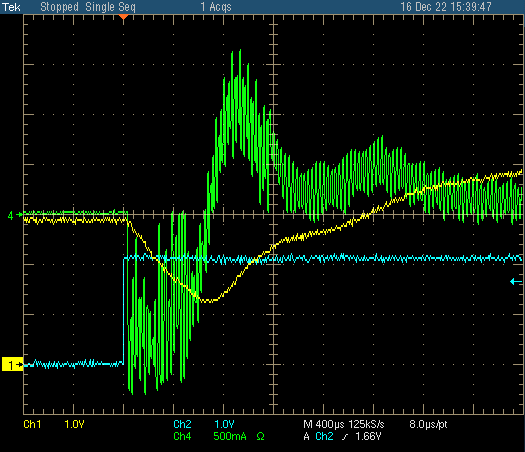
    We took some scope samples with a current probe measuring the inductor current today investigating this case. I found nothing strange on the inductor currents when the ENABLE line was pulled low. When the enable line was released, I could indeed see the negative currents.

    • Blue is the ENABLE pin
    • Yellow is Vout
    • Green is the inductor current
    • Magenta is the PH pin

    Here is a case when the 4V rail was at about 3V (and PH was not measured)

    Here is a case where we let the 4V rail to about 0.1V

    So for the moment we assume that as you mentioned the negative currents could be the cause of the defects.

    We are running another test batch now with extra load connected to discharge the 4V rail capacitors and having a MCU with open drain to pull the enable line low and releasing in between the power cycles to test if we have defects in this scenario and further pinpoint the exact case.

    Best Regards

  • Hi Kurt,

    Thanks for the update. Did you also check in the first case (device disabled when VIN<4V) if there is any damage if the 4V output is not discharged between power cycles? 

    The amount of negative current will depend on the value of the output voltage and the slew rate of VIN. It could be that in some conditions the currents are quite high.

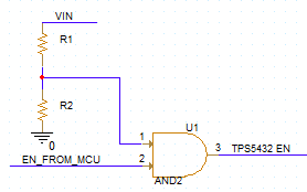
    For your application in case it's important to enable via the MCU, can you think of using an AND gate like below to make sure both conditions VIN>4V and high from MCU are fulfilled before enabling the TPS5432?

    Best regards,

    Varun

  • Dear John,

    On your first question : On the test setup we had before where we let Vout drain completely, no damages were detected. the second test setup where we did not let Vout drain we did have damages. Just to be clear in these test cases, the enable line was never set in the case that Vin < 4V! So we are sure that the problems we are seeing can not be solved by checking Vin as suggested in your last reply.

    Our testing during the weekend as mentioned in my post from friday :

    • Another test batch now with extra load connected to discharge the 4V rail capacitors and having a MCU with open drain to pull the enable line low and releasing in between the power cycles, we dimensioned the load and MCU timing so we can guarantee that the output capacitors are drained of most of its energy:
      • We saw zero defects. We ran this test setup twice as long as all tests before to be sure (friday night and saturday night)
    • We removed the extra load from the 4V on the full test batch and have the same MCU behaviour for one night (sunday night)
      • We again see defects.

    So we are now confident that the defects are caused by draining the 4V output capacitors through the bottom FET.  This seems to me as a design flaw in the device. It is clearly stated in the datasheet that the converter has internal protection to safeguard him from this scenario :

    You can see the 1.8A protection go into action on the captures as shown above, but they seem to be unable to keep the bottom FET safe.

    What is not clear to me, is that the protection works on 1.8A, but the bottom FET specification talks about a maximum current of 1.8A that is typical. The minimum however can be as low as 0.8A! This matches our findings that not all devices are destroyed. Is this 0.8A specification not to low when the current limit is set at 1.8A ?

    In my opinion this is a serious case that means that a DC./DC converter can self destroy every time an enable line is toggled...

    If you would like to reproduce this:

    • We found that a test batch of 20 DUTS should be enough
    • Give a steady input supply of 5V
    • Configure the output to 4V (the higher the output, the more energy in the output capacitor, i assume this would also work with 3.3V out)
    • Provide output capacitor of 100µ-200µF (best to add about 100µF to your TPS5432EVM)
    • Connect no load to the output to not discharge the output and keep the energy available to destroy the bottom FET
    • Pull the EN line low for 100ms every minute as an example schedule

    Best regards

  • Hi Kurt,

    Thanks for the clarification about the tests you ran. Thinking more about it, the negative currents in the startup scope shots you sent seem alright. This is because the internal reference is slowly ramped up to the target 0.808V during soft start, and the control loop will try to regulate the VSENSE voltage to the reference - to do this it has to discharge VOUT. The question is if there is some situation where this negative current is somehow not limited by the negative current limit protection. The negative current limit should work for all conditions where VIN>VOUT and VOUT>VOUT_Target.

    The low side FET in the device has both positive and negative current limits. What's shown in the spec table is the positive current limit. The reverse current limit section also mentions that the negative current limit is around 1.8A. 

    Could you confirm again if there is any negative currents through the low side FET while disabling or ramping the input down when the output is not completely discharged? There is no short on the VIN pin right? Just the PH pin is damaged?

    I shall check these tests out in the lab after the holiday break. 

    Do you want to consider one of our newer devices like TPS62826 for this application?

    Best regards,

    Varun

  • Dear John,

    The negative current limit should work for all conditions where VIN>VOUT and VOUT>VOUT_Target.

    I dont get this VOUT>VOUT_Target condition. Should this current limiter not work under all conditions ?

    Could you confirm again if there is any negative currents through the low side FET while disabling or ramping the input down when the output is not completely discharged?

    Yes, I do not see any problems in the disabling or the ramping the input down. The problem solely comes from enabling the device when there is a remaining charge on the output capacitors.

    There is no short on the VIN pin right? Just the PH pin is damaged?

    That is correct. The defective converters I desoldered all had a short from the PH pin to ground.

    Do you want to consider one of our newer devices like TPS62826 for this application?

    That could be an option. In the past we used the TPS82085SIL converter for this purpose. But since about a year and a half  ago this converter can not be found anymore. We had al lot of stock but since no lead-times given were respected we had to redesign the hardware to a converter that was available at the time. We now have about 600 of these converters already out. So we need to think now about how we can patch up our stock and solve the already delivered products...

    I will keep you posted if I find out anything else that might be of intrest to you.

    Regards

  • Hi Kurt,

    The device should sink negative current only when the feedback voltage (VSENSE) is greater than the internal reference of the error amplifier. When the sensed feedback is higher than the internal reference, the device tries to bring VSENSE to the internal reference voltage by discharging VOUT (sinking negative current). While starting up the device, the internal reference is ramped up slowly during the soft start time to 0.808V. In case VOUT is not completely discharged from the previous cycle, the VSENSE voltage will be greater than the internal reference during startup, and the device should sink negative current till VSENSE = < reference voltage.

    What I meant by VOUT_Target, is the output voltage the device wants to regulate to based on the internal reference voltage and external feedback dividers. Another instance when the actual VOUT can be greater than the target VOUT is when the output load changes suddenly from high load to light load. In this case also there can be some negative currents.

    Best regards,

    Varun